
Samsung Patents a Trick That Cuts Wait Times When Saving Files to Storage
Samsung is patenting a way to make NAND flash storage write data faster by reordering how the storage chip reports back to the device it's connected to.
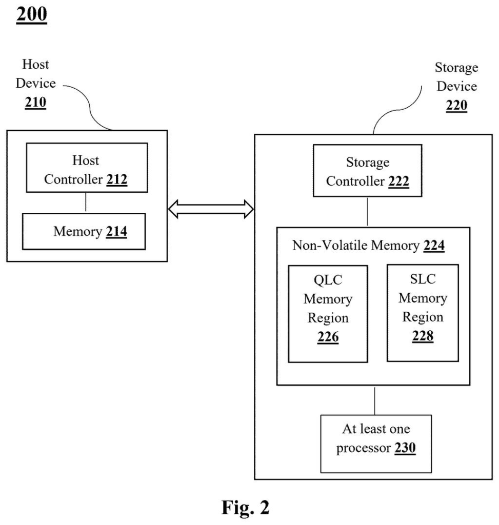
How Samsung's storage write trick actually works
Imagine a courier service that normally waits at your door for a signed receipt before going back to the warehouse to grab your next package. That back-and-forth eats time. Samsung's patent describes doing something similar to telling the courier to skip the signed receipt and go grab the next package while the first one is still being processed.
In storage terms, when your phone or computer sends data to a flash chip to be saved, the chip normally confirms each step is done before asking for the next batch of data. Samsung's approach holds back that confirmation and instead starts pulling in the next chunk of data straight away, keeping the pipeline moving without idle gaps.
The end result is that the storage chip spends less time waiting and more time actually writing, which can make the overall process faster without needing faster hardware.
… preventing a transmission of a first completion indication of the set of operations to the host device …
Translation: The device deliberately delays telling the computer that a save task is finished.
Inside Samsung's pipelined NAND write sequence
NAND flash memory (the type of storage inside SSDs, smartphones, and USB drives) writes data in a fixed sequence of steps called a predefined routine. Normally, after each step completes, the storage controller sends a completion signal back to the host device (your phone, computer, or server) before proceeding. That signal-and-wait pattern creates small idle windows.
This patent describes a method where the storage controller suppresses that first completion signal. Instead of pausing to tell the host "step one is done," the controller immediately starts receiving the next batch of data blocks associated with the following step. The host isn't left waiting for a confirmation that never comes until the full write sequence is further along.
The key steps the patent describes are:
- Receive one or more write commands, each carrying a data block and a destination page in flash memory.
- Start executing the first set of write operations.
- Block the completion acknowledgment from going back to the host.
- Accept the next round of data blocks while the first operations are still wrapping up.
- Execute the subsequent write operations on those incoming data blocks.
This is essentially a write pipeline: overlapping the tail end of one operation with the setup of the next, so the flash memory is kept busy rather than sitting idle waiting for handshakes.
… receiving data blocks associated with each command, the data blocks being associated with a subsequent set of operations of the predefined routine …
Translation: It grabs the next batch of data while it is still handling the previous task.
What this means for SSDs and storage devices
SSD and flash storage performance is often measured in how fast data can be written under sustained load. Reducing idle time between write operations, even by small margins, adds up when a device is handling thousands of write commands per second. This matters most in servers, high-end SSDs, and smartphones doing heavy background tasks like app installs or large file transfers.
For Samsung, which manufactures both NAND flash chips and the controllers that drive them, a firmware-level improvement like this can be shipped as a software update rather than requiring new silicon. That makes it a low-cost way to improve performance numbers on existing hardware, which matters in a competitive SSD market where speed benchmarks drive purchasing decisions.
This is a practical, incremental storage engineering patent rather than anything architecturally new. Pipelining and completion-signal optimization are well-understood techniques in storage design, so Samsung is mostly staking a claim on a specific implementation in NAND controllers. It's not exciting, but it's the kind of quiet work that shows up as a few percentage points better on SSD benchmarks.
There are more where this came from
We read every patent application Big Tech publishes and send you the ones worth knowing. Plain English, free, every week.
The drawings
5 drawing sheets from US 2026/0227913 A1 · click any drawing to enlarge


Want this weekly breakdown for a company we don't cover? Patentlyze Pro →
Be the first to weigh in