
Samsung Patents a Device Housing That Doubles as Its Own Electrical Connector
Samsung has filed a patent for a ring-shaped device housing that physically pokes inward to make electrical contact with the circuit board inside, skipping the separate connector parts that normally take up space.
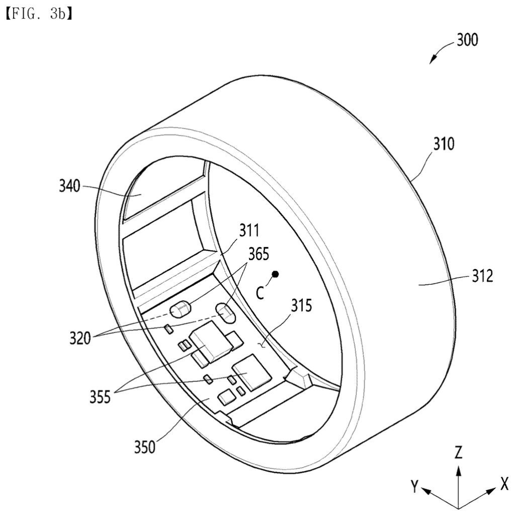
What Samsung's protruding housing actually does inside a device
You're designing a tiny wearable, like a smart ring, and you need electricity and data to flow between the metal outer shell and the electronics inside. Normally that means adding extra connector parts, wires, or contact pads, all of which eat into the already tiny space.
Samsung's patent describes a different approach. The metal housing itself has a small bump, or protruding area, shaped so it presses directly against the circuit board inside. The metal casing stops being just a shell and starts acting as part of the electrical circuit.
The result is fewer separate parts inside a very compact device. That matters most in something like a smart ring, where every fraction of a millimeter of internal space is precious.
How the inward bump bridges the housing and the circuit board
The patent describes an electronic device built around a ring-shaped (annular) housing made from conductive metal. A circuit board sits inside that ring, floating slightly away from the inner wall.
The key detail is a protruding area: a section of the housing's inner surface that is shaped to jut inward toward the board. That protrusion makes direct physical and electrical contact with the board, so current (and potentially data signals) can flow between the outer casing and the internal electronics without a dedicated connector component in between.
The claim is spare on specifics, but the underlying logic is straightforward:
- The housing is both the structural shell and an electrical conductor.
- The protrusion controls exactly where contact is made, replacing a loose wire or a press-fit metal clip.
- Because the housing itself carries the connection, the internal layout can be tighter.
This is a form of structural integration, building a functional component into a part that previously only had a mechanical role. It's a design philosophy common in aerospace and medical devices, and it's starting to appear in consumer wearables where size constraints are extreme.
What this means for small wearables with tight internal space
The device category this patent most obviously fits is the smart ring, a category Samsung has already entered with the Galaxy Ring. Inside a ring, the circuit board, battery, and sensors compete for space measured in millimeters. Removing even one discrete connector component can free up room for a larger battery or an additional sensor.
For everyday users, the payoff would be a device that lasts longer between charges or packs in more health-sensing capability without growing physically larger. The manufacturing angle matters too: fewer parts typically means fewer assembly steps and fewer points where something can come loose over time.
This is the 157th Samsung filing in the chip patents we cover since May, joining earlier ones like one on a GPS accuracy fix and one on AI data storage.
The tradeoff this design makes is subtle but real. When a connector is a separate part, you can tune it precisely for electrical resistance, spring tension, and durability. When the housing itself is the connector, those properties become locked in by the choice of housing material and geometry. If the metal creeps or the protrusion wears down slightly over thousands of daily motions, the contact degrades and there is no easy fix.
For a ring that lives on your finger and flexes with every grip, that wear question deserves serious attention. The patent does not address it, which is typical for a filing at this stage.
Still, the core trade reads as worth exploring. Saving internal volume in a ring-sized device is so valuable that accepting some engineering constraints on the housing material is a reasonable exchange. This is the kind of quiet structural optimization that shows up in mature product lines, not as a headline feature, but as the thing that lets the headline features actually fit inside the device.
There are more where this came from
We read every patent application Big Tech publishes and send you the ones worth knowing. Plain English, free, every week.
The drawings
15 drawing sheets from US 2026/0282251 A1 · click any drawing to enlarge


Want this weekly breakdown for a company we don't cover? Patentlyze Pro →