
Samsung Patents a Camera Chip That Captures Cleaner Photos by Reading Pixels in Shifts
Every digital photo starts as a flood of electrical signals, and noise sneaks in when those signals interfere with each other. Samsung has filed a patent for an image sensor that staggers when different groups of pixels are read out, so that interference has less chance to take hold.
What Samsung's staggered pixel-reading sensor actually does
You're shooting photos at a birthday party, the candles are the only light source, and every shot comes back looking grainy. That grain often has nothing to do with the scene itself. It comes from electrical interference inside the sensor, as millions of pixel readings all try to happen at once.
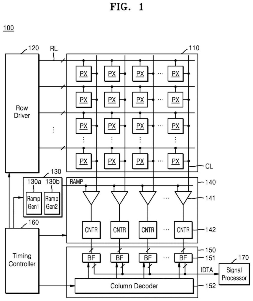
Samsung's patent describes an image sensor that splits the pixel grid into groups and reads each group at a slightly different moment in time. Two separate signal generators take turns, so the comparisons that turn raw pixel charge into usable data are spread out rather than piled on top of one another. Spreading them out reduces how much those comparisons can interfere with each other, which translates to a cleaner image.
This kind of fix happens entirely inside the chip, before your phone ever processes a single pixel. For you as a photographer, it just means better-looking shots in dim or mixed light, without any extra taps or settings.
… a first analog-to-digital conversion (ADC) circuit configured to compare the first ramp signal with a reset signal of a first-first color pixel disposed on the first row and the first column and compare the first ramp signal with a reset signal of a second-first color pixel disposed on the first row and the (N+1)th column …
Translation: It details how specific pixel circuits process light data across arranged grid rows and columns.
How the two ramp generators take turns comparing pixel signals
The patent describes an image sensor built around a pixel array split into two color-pixel groups, arranged in mirrored columns. Think of the sensor as a grid: the left half holds the first color-pixel group, the right half holds the second.
Each group is served by its own ramp signal generator. A ramp signal is a voltage that rises steadily over time. To convert a pixel's light reading into a digital number, a comparator circuit watches for the moment the ramp voltage matches the pixel's own voltage. That crossing point becomes the digital value. Samsung's design uses two generators producing four ramp signals total, so each half of the sensor has its own dedicated source.
The critical detail is timing. The first group's comparisons happen at a different moment than the second group's comparisons. The patent calls these distinct "comparison time points." By staggering when each group does its work:
- Electrical noise that one group generates doesn't land on top of the other group's reading window
- Crosstalk between adjacent columns is reduced
- The reset signals for pixels at the corners of each block are compared independently, not simultaneously
The result is that each analog-to-digital conversion (ADC) circuit, the circuitry that turns a voltage into a number, operates in cleaner electrical conditions than a sensor where all columns fire at once.
The comparing of the first ramp signal occurs at a comparison time point different from a comparison time point during which the comparing of the second ramp signal occurs.
Translation: Different pixel groups are read at separate times to reduce noise in the final image.
What this means for low-light photos on your next Samsung phone
Noise in digital photos is one of those problems that camera manufacturers attack from every angle: bigger pixels, faster processors, AI-based denoising after the fact. This patent targets the problem at the hardware level, before any software ever sees the image. That matters because fixing noise at the source is generally more effective than cleaning it up later, which can soften fine detail.
For Samsung's track record in image-sensor patents, this fits a pattern of incremental but real improvements to the core capture pipeline. You would most likely notice the payoff in the situations where cameras already struggle: candlelit dinners, concerts, indoor sport. Cleaner raw data from the sensor means the phone's processor has more to work with, and AI denoising has less work to undo.
Samsung's 119th filing we've tracked since May in our camera sensor work builds on earlier applications like one catching read errors and one balancing bright and dark scenes.
Samsung's fix here targets a specific moment of electrical chaos inside the sensor: when too many pixel measurements happen at once, they interfere with each other and introduce noise into your photo. The solution splits the sensor into two halves and staggers their timing, so the interference never builds to a critical level.
For most people, this matters most in low light, where sensor noise is the difference between a photo that looks grainy and muddy versus one that holds detail. Software can clean up some noise after the fact, but it cannot fully recover information the sensor failed to capture cleanly in the first place.
The improvement will not be obvious in bright daylight or in a side-by-side comparison between last year's phone and this one. It shows up at the edges of what a camera can do, in dim restaurants or evening outdoor shots, where a cleaner sensor floor means finer detail survives all the way to your screen.
There are more where this came from
We read every patent application Big Tech publishes and send you the ones worth knowing. Plain English, free, every week.
The drawings
16 drawing sheets from US 2026/0281575 A1 · click any drawing to enlarge


Want this weekly breakdown for a company we don't cover? Patentlyze Pro →