
Samsung Patents a Camera Sensor Circuit That Captures Bright and Dark Scenes at Once
Getting a photo that looks right in both the bright sky and the shadowy ground has always been a hardware headache. Samsung's new patent tackles that problem at the chip level, inside the circuit that converts light into digital data.
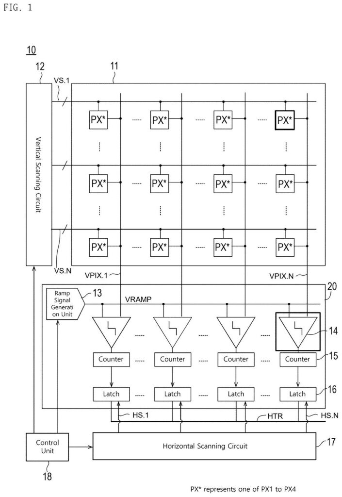
What Samsung's multi-gain image sensor actually does
A smartphone camera points at a window on a sunny day. The sky outside is blown out white, the room inside is nearly black, and no matter what the phone does, it can't make both look right at the same time. That tradeoff has frustrated photographers for decades.
Samsung's patent describes a circuit inside the image sensor itself that handles this by reading each pixel at more than one sensitivity level during a single capture. Instead of one "ear" listening for the light signal, the chip has several, each tuned differently, so it can pick up both the faint whisper of a dark corner and the loud shout of a bright highlight without clipping either one.
The result is that the sensor gathers richer information from a single exposure, giving the camera software more to work with when it reassembles a final image. You'd potentially see less washed-out skies and fewer muddy shadows, especially in challenging mixed-light situations.
a ramp signal input circuit configured to receive a ramp signal and output a ramp-side signal; a plurality of pixel signal input circuits, each configured to receive the analog pixel signal and output a pixel-side signal; …
Translation: The circuit takes in both the reference signal and multiple pixel signals to process the image data simultaneously.
How the comparator switches between pixel input circuits
Image sensors convert light into digital numbers through a process called analog-to-digital (AD) conversion. The traditional approach compares each pixel's raw voltage against a steadily changing reference signal called a ramp signal. When the two match, the circuit records the time, and that timestamp becomes a number representing how bright that pixel is. One comparison, one reading, one sensitivity level.
Samsung's patent redesigns the comparator, the component that makes that comparison, to include a single ramp signal input but multiple pixel signal input circuits. Think of it as a single judge listening to several witnesses at different volumes. Each pixel signal input circuit can be tuned to a different gain (amplification level), so the comparator can effectively read the same pixel at different sensitivities in sequence, or read different pixels optimized for different brightness ranges.
The comparison circuit then picks the result from whichever pixel input circuit is active for a given conversion phase. This hardware arrangement supports what engineers call multi-gain AD conversion, where a sensor captures high-gain data (good for dark areas) and low-gain data (good for bright areas) within the same readout cycle.
- One ramp signal input feeds the comparator
- Multiple pixel signal inputs, each with its own gain setting, connect to the same comparator core
- The comparison circuit selects among them to produce different-sensitivity readings
- Those readings are combined to extend the sensor's effective dynamic range
… a comparator circuit configured to compare the ramp signal input from the ramp signal input circuit with the pixel signal input from one of the plurality of pixel signal input circuits and output a comparison result.
Translation: The core mechanism evaluates the incoming pixel values against a reference level to generate digital values.
What this means for cameras in high-contrast lighting
Dynamic range, the gap between the darkest and brightest detail a camera can capture at once, is one of the last frontiers where smartphone cameras still fall short of human vision. Software tricks like HDR already stitch together multiple exposures, but they can blur moving subjects and introduce artifacts. Doing the same thing in hardware, at the sensor's AD conversion stage, could produce cleaner results with less processing overhead.
For everyday users, a sensor built on this design could handle backlit portraits, sunlit landscapes, and indoor-outdoor scenes with fewer compromises. The approach is also relevant beyond phones: security cameras, automotive cameras, and medical imaging devices all face the same bright-versus-dark challenge. Samsung's interest in image sensor hardware runs deep given its foundry and consumer electronics businesses, so filings in this area tend to track real engineering priorities.
Samsung's 117th filing we've tracked since May in our camera sensor push watchlist builds on a slimmer camera design and an AI photo comparison tool.
Getting this from patent to product requires building a custom chip, not updating an app. The comparator described here is a physical circuit that has to be designed into a sensor from the ground up, which means factory production, device integration, and hardware validation all have to happen before anything ships.
Samsung makes its own image sensors and the devices those sensors go into, so the shortest route to a product runs entirely inside one company. That removes a major obstacle that would slow down any outside licensee trying to use this.
Whether this ends up in a phone camera or a specialized industrial sensor is impossible to say from this filing alone, but the engineering problem it solves, capturing bright and dark parts of a scene accurately at the same time, is one that matters to almost every camera on the market.
There are more where this came from
We read every patent application Big Tech publishes and send you the ones worth knowing. Plain English, free, every week.
The drawings
13 drawing sheets from US 2026/0281590 A1 · click any drawing to enlarge


Want this weekly breakdown for a company we don't cover? Patentlyze Pro →