
Samsung Patents a Way to Route Internal Device Signals Through the Stylus Sensor Layer
Samsung wants the thin grid of coils that senses your stylus to do a second job: carry electrical signals between the processor and other components, cutting down on the cable clutter packed inside modern tablets.
How Samsung's stylus layer pulls double duty inside a tablet
A stylus glides across a tablet screen, and somewhere beneath the glass, a mesh of tiny coils tracks every movement. That sensor layer has always had one job. Samsung is now patenting a way to give it a second one.
Inside phones and tablets, dozens of small components (cameras, sensors, fingerprint readers) need data connections running back to the main processor. Right now, those connections are separate wires routed around the display. Samsung's idea is to run some of those wires through the stylus-sensing layer that already sits under the screen, using the same conductive material that forms the coils.
For you, the payoff is a device that is easier to make thinner or to pack with more components in the same space. Fewer dedicated cables means fewer things fighting for room inside a body that's already incredibly tight.
… a signal line disposed in at least one of the first conductive layer and the second conductive layer, the signal line electrically connecting the electronic module and the processor.
Translation: The patent describes embedding data wires directly into the layers of the stylus sensor to connect internal components.
How the digitizer coil layers carry a second electrical job
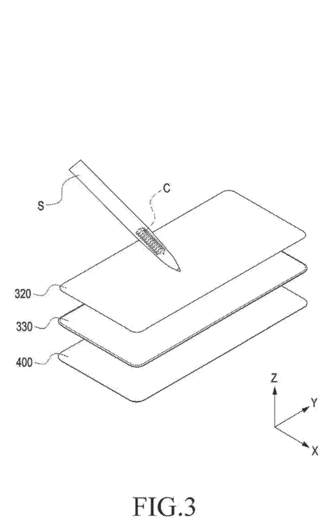
A digitizer is the layer beneath a touchscreen that detects a stylus. It works by sensing the magnetic field changes produced by a stylus tip moving across coils of wire embedded in a conductive layer. Samsung's patent describes a digitizer built from two stacked conductive layers, each carrying a grid of coils oriented in different directions to give precise X and Y position data.
The specific addition here is a signal line etched into one or both of those same conductive layers. That line is not part of stylus detection; it is a dedicated electrical pathway connecting the main processor to an electronic module, a term the patent uses for components positioned around the display panel (think cameras, sensors, or biometric readers).
By embedding that signal line inside the digitizer stack, Samsung avoids routing a separate flexible cable around or under the display assembly. The two conductive layers in the digitizer are:
- First conductive layer: sits closest to the display panel, holds horizontal or vertical coils
- Second conductive layer: sits beneath the first, holds coils in the perpendicular direction
- Signal line: etched into one or both layers, running from processor to peripheral module
The design keeps the stylus-sensing function intact while adding a routing function at essentially no extra thickness cost, because the conductive material was already there.
… the digitizer includes a first conductive layer on which a plurality of first coils are disposed, a second conductive layer on which a plurality of second coils are disposed, wherein the first conductive layer is disposed between the second conductive layer and the display panel …
Translation: This explains the physical layout of the sensor grid that sits underneath the screen to track the stylus.
What this means for thinner Samsung tablets and phones
Thinning a device is mostly a war against thickness budgets. Every cable, every connector, every separate layer adds fractions of a millimeter that compound fast. If Samsung can use a layer that must exist anyway (the digitizer) to carry signals that would otherwise need their own dedicated flex cable, that is a real, if incremental, space saving.
This filing sits squarely in the industrial-design engineering territory that tends to precede new tablet or foldable hardware generations, and it joins a steady flow of new Big Tech patents around display-stack architecture that signal where premium device interiors are heading.
The shortest path from this patent to a shipping product is shorter than most: no new materials, no new manufacturing process, just a rerouted electrical trace on a layer Samsung already makes. The hardware infrastructure needed is essentially whatever Samsung's next digitizer-equipped device is. It reads as an engineering decision already made or being finalized, the sort of detail that shows up in a patent application right as a product generation locks its internal layout.
There are more where this came from
We read every patent application Big Tech publishes and send you the ones worth knowing. Plain English, free, every week.
The drawings
13 drawing sheets from US 2026/0236131 A1 · click any drawing to enlarge


Want this weekly breakdown for a company we don't cover? Patentlyze Pro →
Be the first to weigh in