
Samsung Patents a Slimmer Camera Design That Makes Phone Cameras Thinner
Samsung is rethinking how the circuit board inside a phone camera is built, using two zones of different thickness to squeeze more components into less space.
How Samsung's tiered circuit board shrinks camera bulk
A smartphone sits on a table, and the camera bump on its back catches the light. That raised bump is one of the most complained-about features in modern phone design, and it exists because the electronics behind the lens need somewhere to go.
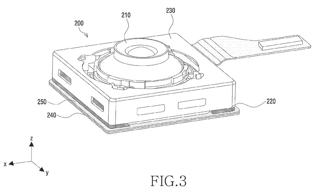
Samsung's patent describes a circuit board inside the camera module that isn't the same thickness all the way across. One zone is thicker and supports the lens and image sensor on top. The other zone is deliberately thinner, and that thinner section has a free face on the underside where extra electronic components can be mounted. Instead of stacking everything vertically and forcing the whole assembly to be taller, the design spreads components sideways into the gap created by the thinner region.
The practical goal is a camera module that takes up less vertical room inside the phone, which could let manufacturers either reduce the camera bump or reclaim that space for a bigger battery.
… wherein the printed circuit board includes a first region having a first thickness, and a second region having a second thickness greater than the first thickness …
Translation: The circuit board has uneven thickness to save valuable space inside the phone.
How the two-zone PCB tucks components out of the way
The patent describes a camera module built around a printed circuit board (PCB) that has two distinct zones: a first region with a thinner profile, and a second region with a thicker profile.
The lens assembly and image sensor (the part that converts incoming light into digital data) sit on the top face of the PCB, which the patent calls the first side. In a conventional camera module, electrical components like capacitors or driver chips are typically stacked in the same vertical column, adding height to the whole assembly.
Here, the thinner first region exposes a second face on the underside of the board. Electrical elements are mounted there instead, tucking into the gap between the bottom of the thin zone and the base that the board rests on. The thicker second region provides the structural depth the lens assembly needs without forcing the entire board to be that tall everywhere.
- Housing holds and protects the overall module
- Lens assembly and image sensor sit on the top (first side)
- PCB thins out in one zone, opening an underside face
- Electrical components mount to that underside, using otherwise dead space
- A base sits beneath the whole PCB assembly
What slimmer camera modules could mean for your next phone
The camera bump on modern smartphones has grown taller each product generation as sensors and lenses get bigger. Any engineering approach that lets the surrounding electronics take up less vertical space gives phone makers a real choice: flatten the back or use the reclaimed room for a larger battery.
For you as a buyer, that could mean a phone that sits flat on a table again or one that simply lasts longer on a charge. The design itself is not exclusive to phones either; it could apply to compact cameras, laptop webcams, or any device where a thin camera housing is desirable. Whether Samsung builds this into a shipping product is a separate question, but Samsung's interest in camera module miniaturization shows up consistently across its patent activity.
That makes this Samsung's 116th filing we've tracked since May on our camera sensor push, joining the one comparing photos with AI and the display that shoots HDR.
Making a circuit board intentionally thinner in one zone and thicker in another is harder to manufacture reliably than a uniform board, and the boundary between those two zones is a natural stress point in a device that spends years getting dropped and overheated. That is the real cost Samsung is accepting here.
The space savings are genuine: tucking components into the vertical gap beneath the thinned area beats bolting on a separate board. But if the footprint of that two-zone board grows sideways to make room for both regions, the phone's internal layout has to absorb that width somewhere.
The logic holds up better than the execution risk does. The idea is sound, the manufacturing gamble is real, and whether the slimmer camera is worth the trickier production line depends entirely on yield numbers a patent cannot provide.
There are more where this came from
We read every patent application Big Tech publishes and send you the ones worth knowing. Plain English, free, every week.
The drawings
16 drawing sheets from US 2026/0282235 A1 · click any drawing to enlarge


Want this weekly breakdown for a company we don't cover? Patentlyze Pro →