
Sony Patent Embeds Math Into Image Sensors to Shrink AI Cameras
Sony is working on an image sensor that can do arithmetic on its own, before any data ever leaves the chip. The math happens inside the pixel itself, using nothing but electrical charge and a capacitor.
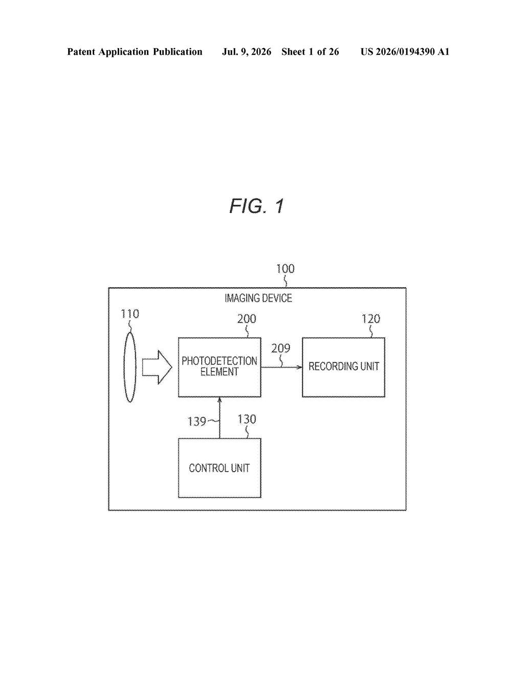
What Sony's in-pixel calculation trick actually does
Imagine your phone's camera could do basic math the moment light hits the sensor, without sending any data to the main processor first. That's the idea behind this Sony filing.
Normally, a camera sensor just captures light and hands raw data off to a separate chip to process. Sony's design lets each pixel perform a simple multiplication on its own, by reading its electrical charge a specific number of times. The number of reads is the multiplier. More reads, bigger number. Fewer reads, smaller number.
This approach uses analog electrical signals rather than digital code, which means the math happens faster and with far less physical space than a traditional arithmetic unit would require. The goal is to shrink the hardware needed to run certain calculations, which is increasingly important as cameras are asked to do things like detect objects or recognize faces the instant a frame is captured.
How the readout circuit multiplies by repeating charge reads
The patent describes an image sensor architecture that performs analog multiplication directly at the pixel level, without converting signals to digital first.
Each pixel contains a photoelectric conversion element (a light-sensitive component that turns incoming photons into electrical charge) and a readout circuit built around a capacitor. That capacitor holds a voltage level proportional to how much light hit the pixel.
The clever part is the arithmetic circuit. Instead of reading the capacitor's voltage once, as a conventional sensor would, this circuit reads it multiple times. The number of reads is controlled by an arithmetic coefficient, essentially the value you want to multiply by. The circuit reads both the baseline "reset" voltage and the light-induced voltage the same number of times, then computes the difference. Repeating those reads effectively scales the signal.
The result is a form of in-sensor compute: multiplication done in analog hardware, at the source, using only capacitors and a counter. No separate digital multiplier unit is needed, which is why Sony claims the design enables further size reduction.
What this means for tiny AI-enabled cameras
As AI features like real-time object detection get pushed into cameras on phones, security devices, and industrial sensors, the bottleneck is often moving data from the sensor to a processor. If the sensor can handle some of the math itself, you get faster results and a smaller, lower-power chip overall.
Sony is one of the world's largest image sensor manufacturers, supplying chips to Apple and many other device makers. A patent that shrinks the compute footprint of AI inference inside a sensor is directly relevant to where the industry is heading: smaller cameras, faster frame analysis, and less reliance on a big external processor to do the heavy lifting.
This is a genuine engineering idea, not a vague concept. Analog in-sensor compute is a real research direction, and Sony's specific mechanism (controlling multiplication through readout count) is concrete and testable. It won't make headlines the way a new iPhone camera feature does, but it's the kind of foundational work that shows up in next-generation sensor silicon a few years from now.
Get our take in your Top Stories
Liked this breakdown? Add Patentlyze as a preferred source on Google, and our plain-English take shows up more often in your Top Stories the next time Sony patent news breaks.
There are more where this came from
We read every patent application Big Tech publishes and send you the ones worth knowing. Plain English, free, every week.
Want this weekly breakdown for a company we don't cover? Patentlyze Pro →