IBM Patents a Vertically Stacked P-N Diode Built Into FET Gate Structures
IBM has filed a patent for a P-N diode that lives inside the same physical space as a transistor's source and drain regions — stacking two oppositely doped semiconductor layers vertically rather than side by side. It's a geometry trick that could matter a lot as chip features keep shrinking.
What IBM's stacked diode inside a transistor actually does
Imagine trying to fit two different rooms into the same square footage of an apartment — you don't expand sideways, you build up. That's essentially what IBM is doing here with a key component inside a computer chip.
A P-N diode is one of the most basic building blocks in electronics — it controls which direction electricity can flow. Normally, building one next to a transistor (the on/off switch on a chip) takes up extra horizontal space on the silicon. IBM's approach instead stacks the two halves of the diode — one P-type (positive carrier) layer and one N-type (negative carrier) layer — on top of each other, tucked into the recessed pockets between gate structures called source/drain canyons.
The result is a diode that occupies no extra footprint on the chip's surface. For engineers designing ever-smaller transistors, that's a meaningful efficiency gain — you get the protection and current-control functions of a diode without sacrificing precious chip real estate.
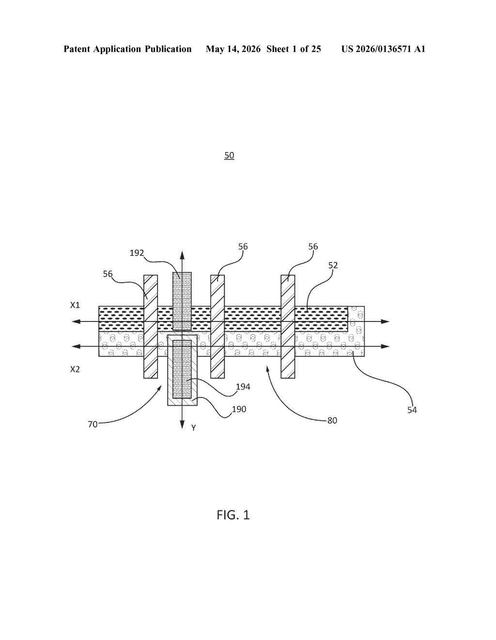
How IBM stacks P-type and N-type regions in source/drain canyons
The patent describes a semiconductor device built around standard FET (field-effect transistor) gate structures — the kind of architecture used in modern FinFET and gate-all-around (GAA) chip designs. Between those gate structures are recessed pockets called source/drain canyons, which normally hold the epitaxial (crystalline semiconductor) material that feeds current into the transistor channel.
Instead of using that canyon space purely for transistor source/drain material, IBM's design integrates a full P-N junction (the core of a diode) directly inside it. The junction consists of:
- A first epitaxial region of one carrier type (either P-type, which uses "holes" as charge carriers, or N-type, which uses electrons)
- A second epitaxial region of the opposite carrier type, grown directly on top of and in contact with the first
The vertical stacking is the key innovation here. Traditional co-integration of diodes and transistors often requires lateral (side-by-side) separation, which consumes chip area. By growing the two doped layers sequentially in the same trench, IBM eliminates that lateral footprint entirely.
The epitaxial growth process — where atoms are deposited layer by layer in a crystalline pattern — allows precise control over the thickness and doping concentration of each region, which determines the diode's electrical characteristics like breakdown voltage and forward voltage drop.
What this means for shrinking chips without losing diode function
As transistors continue shrinking toward the 2nm node and beyond, every square nanometer of chip area is contested. Electrostatic discharge (ESD) protection diodes, clamping diodes, and rectifiers all need to live somewhere on a chip — and the conventional answer of placing them adjacent to transistors gets harder to justify at extreme scales. IBM's stacked approach offers a way to keep those functions without a separate area budget.
For IBM specifically, this fits neatly into its work on gate-all-around nanosheet transistors, where the source/drain canyon geometry is already a central feature of the architecture. If this integration scheme proves manufacturable, it could influence how ESD protection and power management circuits are laid out in future high-density chips — including server processors and AI accelerators where IBM competes.
This is a solid incremental advance in semiconductor integration, not a headline-grabbing leap. The idea of vertically stacking doped regions isn't new in principle, but applying it specifically to the source/drain canyon geometry of modern FET architectures is a genuinely practical refinement. It's the kind of quiet, structural patent that shows up in real silicon a few process generations later.
Get one Big Tech patent every Sunday
Plain English, intelligent commentary, no hype. Free.
Editorial commentary on a publicly published patent application. Not legal advice.