
Samsung Patent Merges Touch Sensors Directly Into Display Power Supply Layer
Samsung Display is patenting a screen construction where touch-sensing electrodes share the same physical layer as the electrodes that power the pixels themselves. It's a structural simplification that could matter most for the giant tiled screens Samsung sells to venues and businesses.
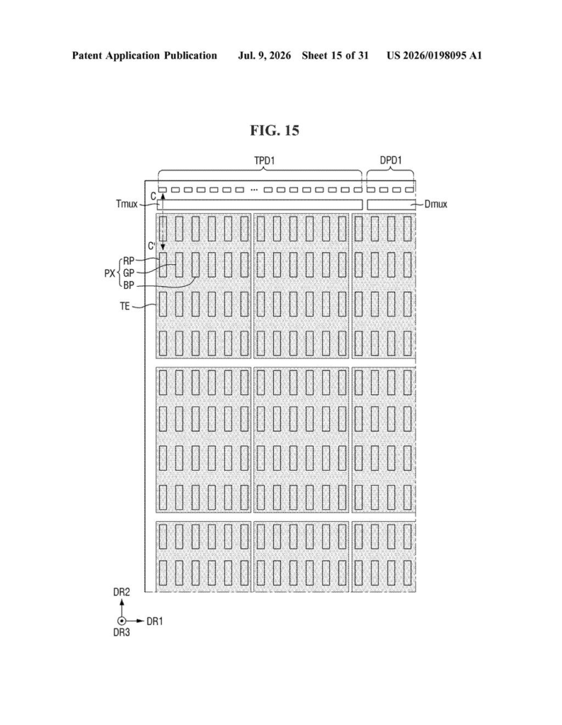
What Samsung's shared-layer screen design actually does
Imagine a sandwich. A regular display screen is built like many thin slices of bread stacked on top of each other, each layer doing a different job: driving the pixels, sensing your touch, carrying power. Every extra layer adds thickness, cost, and potential failure points.
What Samsung is patenting here is a way to combine some of those layers. Specifically, the touch-sensing electrodes (the parts that detect your finger) would be made from the same material and sit on the same level as the electrodes that connect the pixels to their power supply. Instead of a separate dedicated touch layer, you get one layer doing double duty.
The patent covers both single display panels and tiled displays, which are large screens assembled by snapping many smaller panels together side by side, the kind you see on arena scoreboards or large video walls. Reducing layers in those setups can make the seams between tiles less visible and the overall build simpler to manufacture.
How the electrode and touch layers share one material level
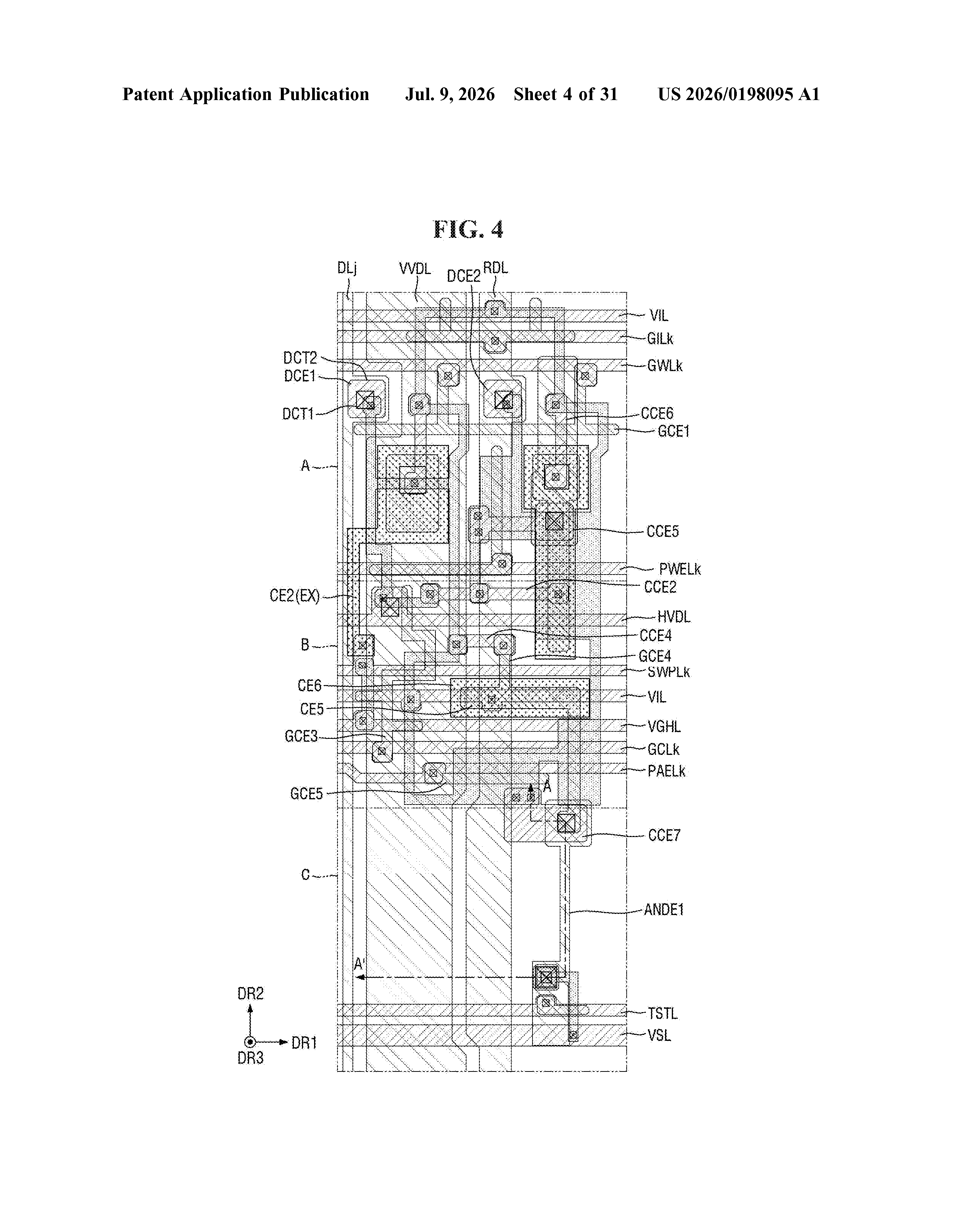
The patent describes a display stack built on a substrate (the base material), with transistors (the tiny switches that control each pixel) sitting above it. On top of the transistors is a first organic insulating layer, an electrically non-conductive plastic-like film that separates the transistors from the wiring above them.
Above that insulating layer, the patent places three things at essentially the same level:
- A first connection electrode that links to the transistors below and ultimately drives the light-emitting element (the pixel itself)
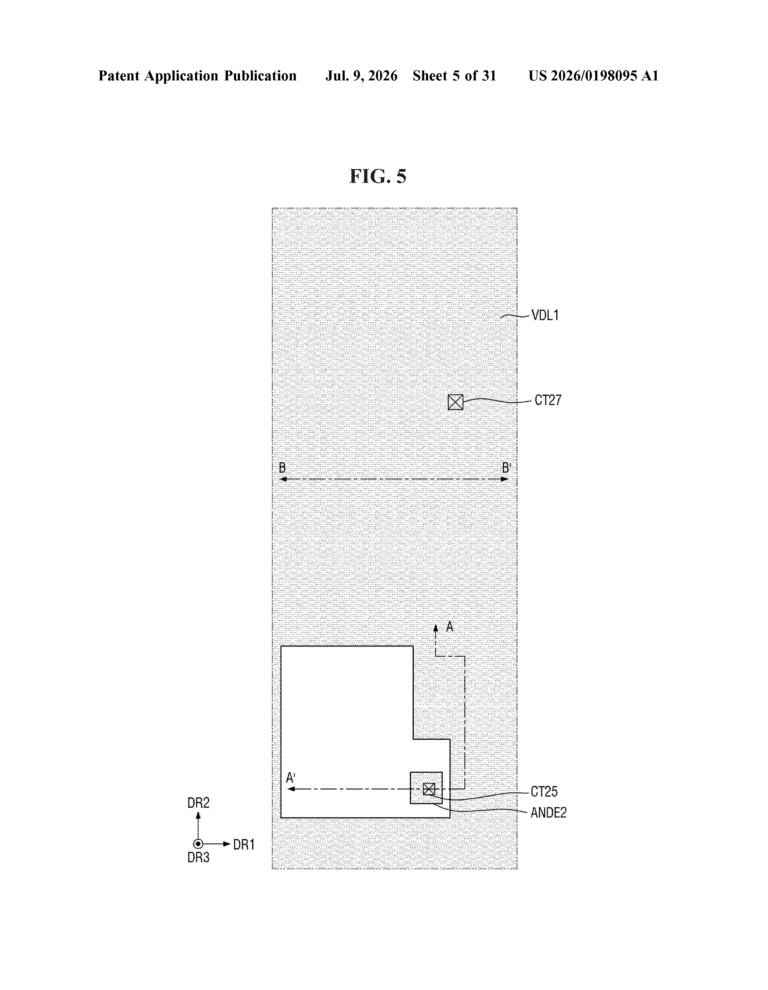
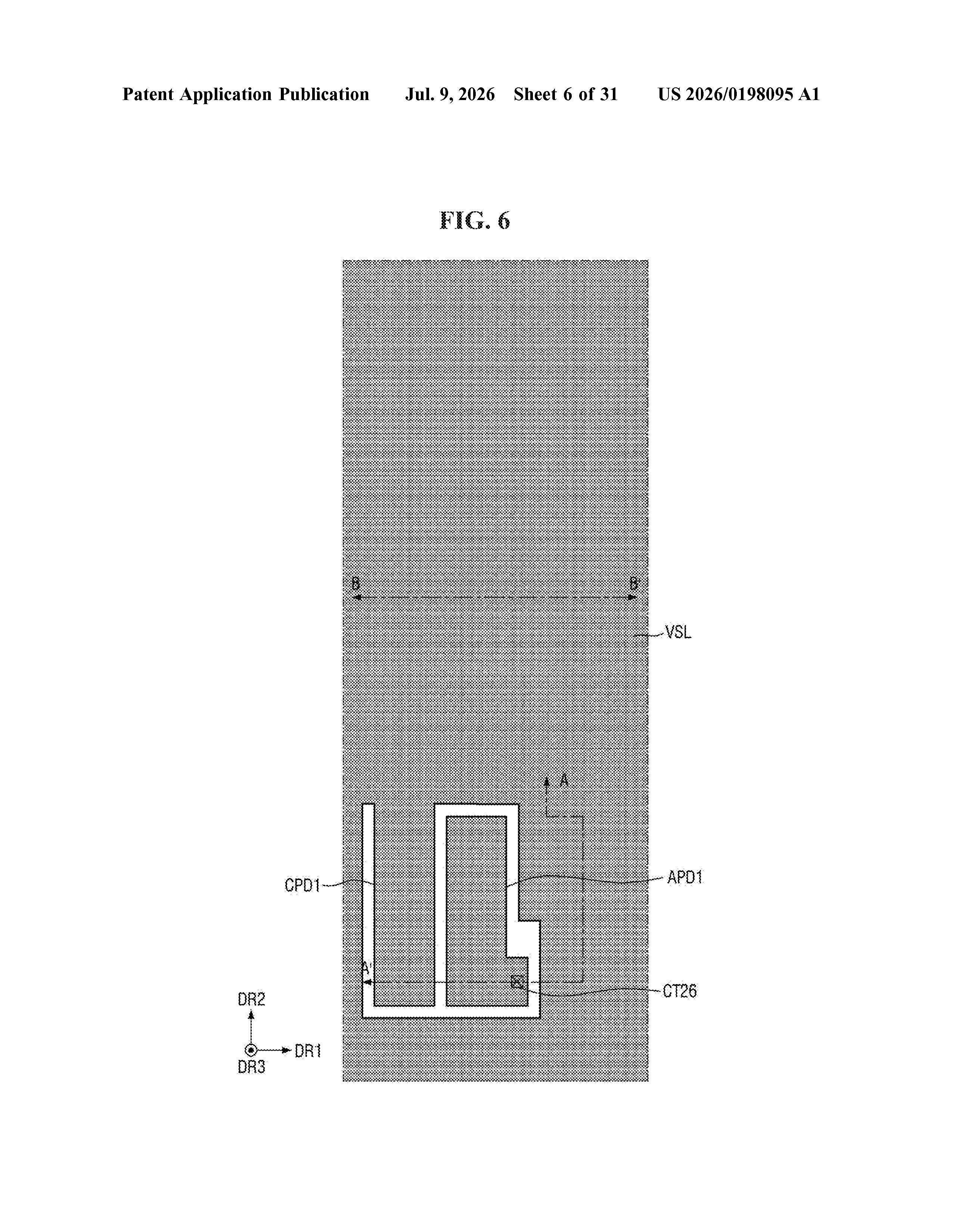
- A second connection electrode connected to a power supply line that feeds voltage to the pixels
- A touch electrode made of the same material as those two connection electrodes
A second organic insulating layer sits above the power supply line and includes an opening area, a deliberate gap that exposes the power line so it can make contact with components above.
The key claim is that the touch-sensing layer does not require its own separate deposition step; it is patterned from the same conductive material deposited for the pixel connection electrodes. That reduces the total number of manufacturing steps and potentially the overall panel thickness.
What this means for large tiled display panels
For tiled display systems, where dozens of panels are assembled edge to edge into one large screen, even small reductions in layer count can meaningfully lower production costs and reduce the risk of defects at the seams. Thinner, simpler panels are also easier to install and maintain in commercial settings like stadiums, retail environments, and broadcast studios.
For consumers, the more immediate question is whether this approach could eventually show up in televisions or monitors where touch capability is still relatively rare because adding a touch layer traditionally adds cost and thickness. If Samsung can fold touch sensing into layers that already exist, the cost barrier to touchscreen TVs or large-format interactive displays drops a little. That's not guaranteed from a patent alone, but it's the direction this points.
This is a manufacturing efficiency patent, not a headline product feature. It won't make screens look better or respond faster in any way a user would notice directly. But for Samsung's commercial display business, which sells large tiled video walls to venues worldwide, shaving fabrication steps out of the stack is real money. Worth a mention, not worth excitement.
Get our take in your Top Stories
Liked this breakdown? Add Patentlyze as a preferred source on Google, and our plain-English take shows up more often in your Top Stories the next time Samsung patent news breaks.
There are more where this came from
We read every patent application Big Tech publishes and send you the ones worth knowing. Plain English, free, every week.
The drawings
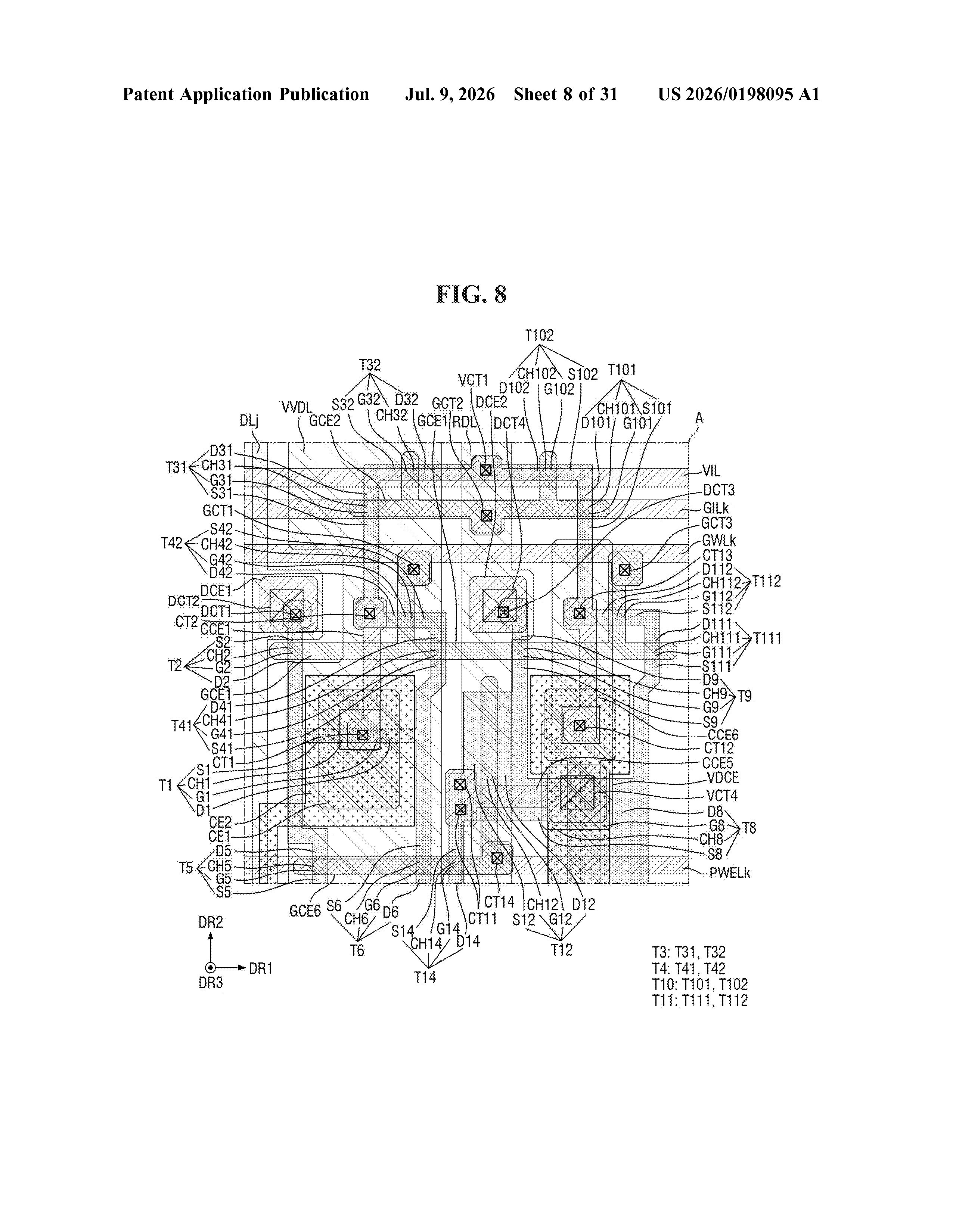
31 drawing sheets from US 2026/0198095 A1 · click any drawing to enlarge
Want this weekly breakdown for a company we don't cover? Patentlyze Pro →