Samsung Patents a Memory Chip That Automatically Moves Data Between Fast and Slow Storage
Samsung is patenting a memory chip that watches how often data gets used — and quietly shuffles it between fast on-chip memory and slower external storage without the processor having to ask.
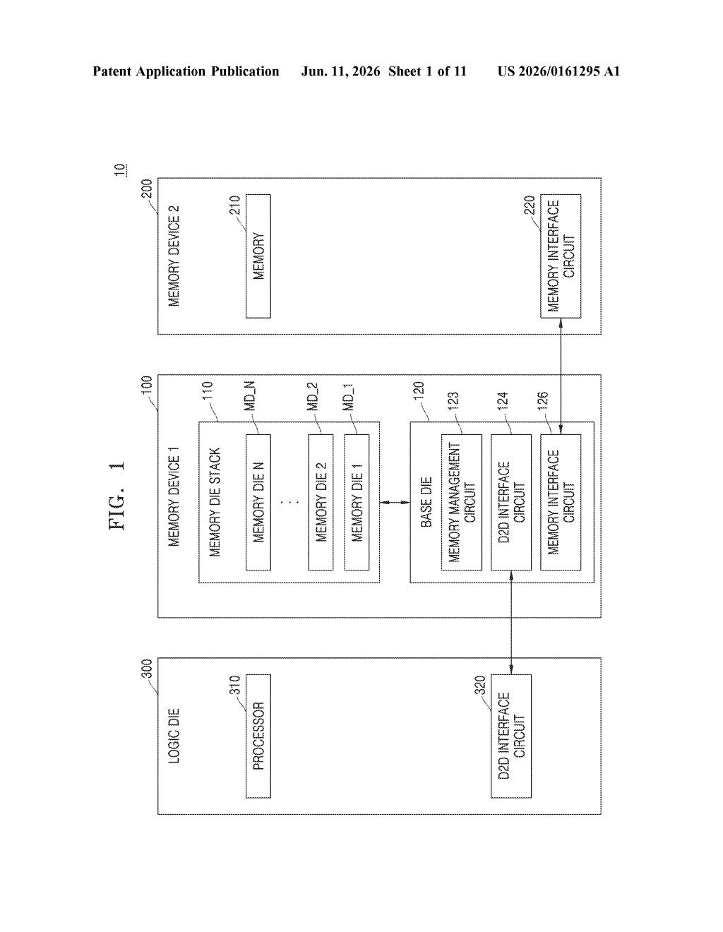
What Samsung's self-managing memory tier actually does
Imagine your home has a desk right next to you and a filing cabinet across the room. You keep the documents you use every hour on the desk, and everything else goes in the cabinet. Now imagine a smart assistant who watches what you reach for and automatically moves papers between desk and cabinet before you even ask. That's the core idea here.
Samsung's patent describes a memory chip with a built-in "base die" — a management layer that sits underneath a stack of fast memory chips. That base die watches which data is being accessed frequently and which is sitting idle. Data that hasn't been touched in a while gets quietly offloaded to a larger, slower external memory module to free up the fast tier. When the processor suddenly needs something that's in the slow tier, the base die fetches it and delivers it directly.
You — or rather the server running your AI model — never has to manually manage any of this. The chip handles the traffic itself.
How the base die decides what data to move and when
The patent describes a stacked memory device built around two main components: a memory die stack (multiple layers of fast memory chips piled on top of each other) and a base die sitting underneath that does all the heavy lifting.
The base die contains four key circuits:
- Via interface circuit — connects the base die upward to the fast memory stack through tiny vertical channels called through-silicon vias
- Die-to-die (D2D) interface circuit — connects the base die to an external processor, so they can talk directly
- Memory interface circuit — connects the base die outward to a separate, larger external memory device (slower but with more capacity)
- Memory management circuit — the decision-making brain that tracks access patterns and decides what to move where
The memory management circuit monitors access information — essentially a running log of how frequently and recently each piece of data has been touched. If data in the fast stack hasn't been accessed in a while, the circuit migrates it out to the external memory to make room. When the processor requests data that's currently sitting in that external memory, the base die retrieves it and serves it directly to the processor without requiring the processor to manage the handoff itself.
This is a form of hardware-managed tiered memory — the intelligence is baked into the chip, not delegated to software.
What this means for AI servers and high-bandwidth memory
AI training and inference workloads are brutally demanding on memory. Large language models need enormous amounts of data close to the processor, but fast memory (like HBM — high-bandwidth memory) is expensive and physically limited in how much you can pack in. Systems today often rely on software to manually manage which data lives where, which adds latency and complexity.
A chip that handles its own data migration in hardware could make AI accelerators and data-center processors meaningfully more efficient without requiring software changes. For Samsung, this is also a competitive play: the company is a major supplier of both HBM and DRAM, and a memory device that intelligently bridges the two tiers could be a compelling product for the AI chip ecosystem — particularly as competitors like SK Hynix and Micron push their own next-generation memory architectures.
This is unglamorous but genuinely useful work. Hardware-managed memory tiering removes a real bottleneck in AI infrastructure, and putting the intelligence in the base die rather than software is an elegant approach. It's not a consumer story — nobody's phone will ever care about this — but for anyone building or buying AI servers, it's the kind of low-level improvement that compounds into meaningful gains.
Get one Big Tech patent every Sunday
Plain English, intelligent commentary, no hype. Free.
Editorial commentary on a publicly published patent application. Not legal advice.