
Samsung
Samsung · Display · Filed Apr 17, 2025 · USPTO published Jun 11, 2026 · Jun 11 release
Samsung Display Patents a Wiring Layout That Keeps Pixel Connections from Overlapping
Deep inside every display panel, millions of tiny transistors need to be wired up without creating electrical interference — and Samsung has filed a patent for a specific way to keep those connections from piling on top of each other.
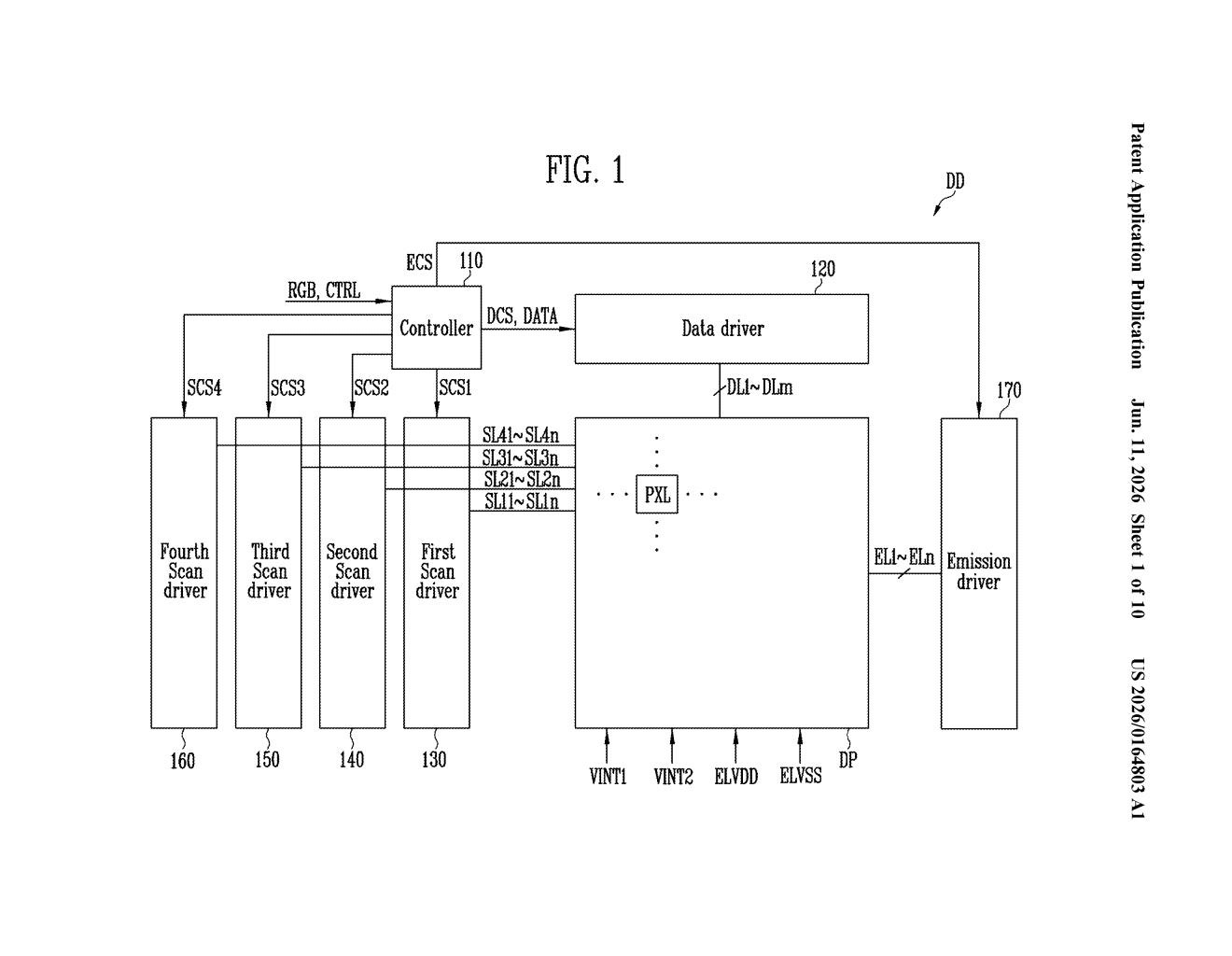
- Publication number
- US 2026/0164803 A1(US20260164803A1)
- Applicant
- Samsung Display Co., Ltd.
- Filed · Published
- Apr 17, 2025 · Jun 11, 2026
- Inventors
- Jong Hyun CHOI, Min Jeong OH
- Status when we published
- Waiting for an examiner
- Document
- 18 claims
- US classification
- 257/499
What Samsung's non-overlapping pixel wiring actually does
Imagine a very crowded apartment building where every resident needs their own dedicated mailbox, but all the mailboxes are stacked in the same narrow hallway. If two packages arrive at the exact same spot at the same time, things get jammed. Something similar happens inside display panels when electrical connections line up directly on top of each other — it can cause reliability problems or manufacturing defects.
Samsung's patent describes a wiring arrangement where two critical connection points are deliberately placed so they don't overlap. One connection point sits where the transistor meets its electrode; the other sits where the data line — the wire that tells each pixel what color to be — hooks into the circuit. By offsetting these two junction points, the design avoids stacking stress in the same physical spot.
This kind of structural detail sounds dry, but it matters at the manufacturing stage. Keeping connections spatially separated can reduce the chance of electrical shorts or failures, which in turn can improve display yield — meaning more panels come off the production line working correctly.
How Samsung staggers the contact points across layers
The patent describes an internal wiring stack inside a display panel, built up in distinct layers. The key components are:
- A second semiconductor pattern — the active channel of a transistor that controls a pixel
- A first second-transistor electrode — an electrode that connects to that semiconductor, running perpendicular to it (meaning it approaches from above rather than from the side)
- A second conductive layer — an intermediate conductor sitting on top of that electrode
- A first bridge pattern — a short conductive bridge on top of that layer
- A data line — the signal-carrying wire that finally connects to the bridge pattern
The critical rule in the claim is spatial: the spot where the transistor electrode meets the semiconductor (first area) and the spot where the data line meets the bridge pattern (second area) must not occupy the same footprint when viewed from above.
In display engineering, overlapping contact regions can concentrate mechanical stress during fabrication and increase the risk of electrical leakage between layers. Staggering these regions distributes that stress and keeps each junction electrically isolated from the other.
What this means for future Samsung display panels
For Samsung Display — which supplies OLED panels to Samsung's own phones as well as Apple's iPhones — manufacturing yield is everything. Even a small improvement in the percentage of defect-free panels produced per wafer translates into significant cost savings at scale. A wiring layout that reduces the risk of layer-to-layer shorts or stress fractures can quietly make panels cheaper to produce without changing anything the end user would notice on a spec sheet.
This patent doesn't hint at a flashy new feature you'd see in a product listing. It's the kind of foundational process patent that protects a specific way of building displays — the sort of IP that matters most in highly competitive panel manufacturing, where Samsung and rivals like LG Display and BOE are constantly racing to improve yields and lower costs.
Source: US 2026/0164803 A1 at the USPTO (PDF). Full patent text and figures are in the official publication.
Get our take in your Top Stories
Liked this breakdown? Add Patentlyze as a preferred source on Google, and our plain-English take shows up more often in your Top Stories the next time Samsung patent news breaks.
Add Patentlyze on Google
One click.
There are more where this came from
We read every patent application Big Tech publishes and send you the ones worth knowing. Plain English, free, every week.
More from Samsung
All 1,629 Samsung patents →
More in Display
All 730 Display patents →
Microsoft
Microsoft Patents a Display Film That Absorbs Specific Colors on Demand

Sony
Patent Targets the Invisible Errors That Corrupt Color and Detail in Digital Photos

Sony
Sony Files Patent to Accurately Reproduce Camera Colors Across Any Display

Sony