Samsung Patents a Camera Chip Design That Shields Its Own Light-Capturing Circuits
Samsung's latest patent quietly addresses one of the most tedious — but consequential — problems in camera sensor manufacturing: keeping a tiny internal electrode from getting damaged during production.
What Samsung's protective gate layer actually does
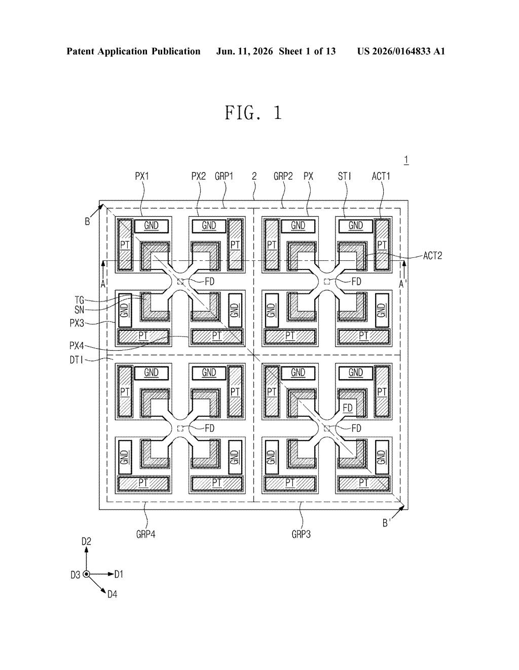
Picture the image sensor in your phone's camera as a grid of millions of tiny light-catching buckets. Each bucket has a little gate — a microscopic electrode — that opens and closes to let the captured light signal pass through. That gate has to be built into the sensor chip itself, which means it sticks up slightly from the surface and can get nicked, contaminated, or misaligned during the manufacturing steps that follow.
Samsung's patent describes adding a protective cap around each of those gate electrodes. The cap sits flush with the chip's surface and is deliberately wider than the electrode it's guarding, so it physically shields the electrode from whatever processes come next.
The sensor itself is designed to receive light from the back side of the chip — a well-established technique that improves low-light performance. The protective pattern is essentially a manufacturing safeguard layered on top of that architecture, aiming to keep these delicate structures intact from the factory floor to your camera.
How the protective pattern wraps the transfer gate electrode
The patent describes a back-side illuminated (BSI) image sensor — meaning light enters from the back of the silicon wafer rather than the front, which improves how much light each pixel can capture.
On the front side of the chip (opposite to where light enters), each pixel has a transfer gate electrode — a component that physically moves the electrical charge generated by incoming light toward the readout circuitry. Part of this electrode sits inside a trench carved into the substrate; another part protrudes above the surface.
The key innovation here is a protective pattern — a structured material layer placed around each transfer gate electrode. The patent specifies that this protective layer must be:
- Flush with the substrate's front surface (so it doesn't introduce height inconsistencies)
- Wider than the protruding part of the electrode it surrounds (so it provides a physical buffer zone)
- Positioned between adjacent pixel regions that are isolated by a full-depth separation structure (a wall that runs all the way through the chip to prevent light or charge from bleeding between pixels)
The geometry — specifically that the protective pattern is wider than the electrode at the surface level — is the claim Samsung is staking out. It's a structural design choice aimed at reducing defects introduced during back-end fabrication steps.
What this means for Samsung camera sensor reliability
Image sensor yield — how many usable chips come off a production line — is one of the biggest cost drivers in smartphone camera hardware. A design that reduces damage to fragile gate electrodes during manufacturing could meaningfully improve that yield, which eventually filters down to either lower costs or higher volumes for high-end sensors.
For Samsung specifically, this matters because the company both makes sensors for its own Galaxy phones and sells them to other phone makers. Incremental reliability improvements in sensor architecture are the kind of quiet, compounding advantages that add up over millions of units. This isn't a flashy new camera feature — it's the unglamorous engineering that makes flashy camera features possible at scale.
This is deep-in-the-weeds semiconductor process engineering — the kind of patent that matters enormously to a fab engineer and almost not at all to a consumer. It signals that Samsung is actively iterating on BSI sensor construction at the structural level, which is worth noting for anyone tracking the company's sensor roadmap, but it's not a harbinger of any specific new camera capability you'll read about in a phone review.
Get one Big Tech patent every Sunday
Plain English, intelligent commentary, no hype. Free.
Editorial commentary on a publicly published patent application. Not legal advice.