Samsung Patents a Memory Layout Designed to Feed AI Chips Faster
Samsung is patenting a way to organize memory so that AI processors spend less time hunting for data — by wiring the memory layout directly to how AI workloads actually read and write information.
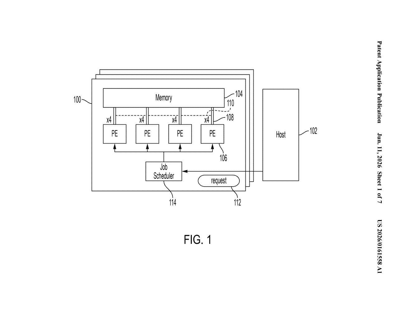
What Samsung's AI-focused memory mapping actually does
Imagine a library where books are shelved in a completely different order from how readers request them — so every lookup requires a slow, manual search. That's roughly what happens when a traditional memory system tries to serve a modern AI chip. The chip asks for data constantly, and if the memory isn't organized to match those requests, the chip sits idle waiting.
Samsung's patent describes a way to lay out memory so each processing engine — a mini-processor dedicated to running AI tasks — gets its own dedicated slice of memory and its own dedicated lanes (called channels) to reach it. When an AI job comes in with a memory address, the engine can figure out exactly where that data lives and pull it through the right lanes without competing with other engines.
The key trick is called interleaving: rather than filling one memory bank at a time, addresses are spread across all the memory units in a repeating pattern. That means workloads that touch lots of memory locations at once — exactly what AI models do — can pull data from multiple places in parallel instead of forming a bottleneck.
How interleaved addresses and channels move AI data
The patent describes a memory system built around interleaved address mapping — a technique where consecutive memory addresses don't sit next to each other in one bank, but are instead spread (interleaved) across multiple memory units in a round-robin fashion. This is similar to how a card dealer distributes a deck evenly around a table rather than giving one player all the cards first.
Each processing engine in the system is paired with one memory unit and a fixed set of channels (the physical data pathways between the processor and memory). The size of each memory unit is deliberately set to match the number of channels assigned to its engine — so the bandwidth available always fits the data region being served.
When an AI operation arrives, the processing engine:
- Receives a request that includes a memory address (a pointer to where the needed data lives)
- Translates that address into a precise physical memory location within its own memory unit
- Pulls the data through one or more of its dedicated channels
- Runs the AI computation on the retrieved data
By keeping each engine's data access local to its own memory unit and channels, the design avoids the traffic jams that occur when multiple processors compete for shared memory bandwidth — a chronic problem in large AI inference and training workloads.
What this means for Samsung's AI chip ambitions
AI models are hungry for memory bandwidth — the speed at which data moves between storage and processors is often the main bottleneck in both training large models and running them in real time. Samsung, as the world's largest memory chip maker, has a direct commercial interest in solving this at the hardware level rather than leaving it entirely to software optimizations.
This patent positions Samsung to offer memory modules that are co-designed with AI accelerators, rather than selling generic DRAM that AI chips have to work around. If this architecture makes it into products like HBM (High Bandwidth Memory) or next-generation processing-in-memory chips, it could let Samsung compete more directly with companies like SK Hynix and Micron on AI-specific memory performance — not just raw capacity.
This is solid infrastructure engineering, not a flashy consumer feature — but it's exactly the kind of unglamorous work that determines whether a company's AI chips are competitive or not. Samsung filing this in late 2025 signals they're serious about baking AI-aware memory organization into silicon, not just marketing existing products as 'AI-ready.'
Get one Big Tech patent every Sunday
Plain English, intelligent commentary, no hype. Free.
Editorial commentary on a publicly published patent application. Not legal advice.