IBM Patents a Storage Drive That Runs Its Own AI Computations
IBM wants to move the AI math closer to where the data lives — inside the storage unit itself — so the main processor doesn't have to do all the heavy lifting.
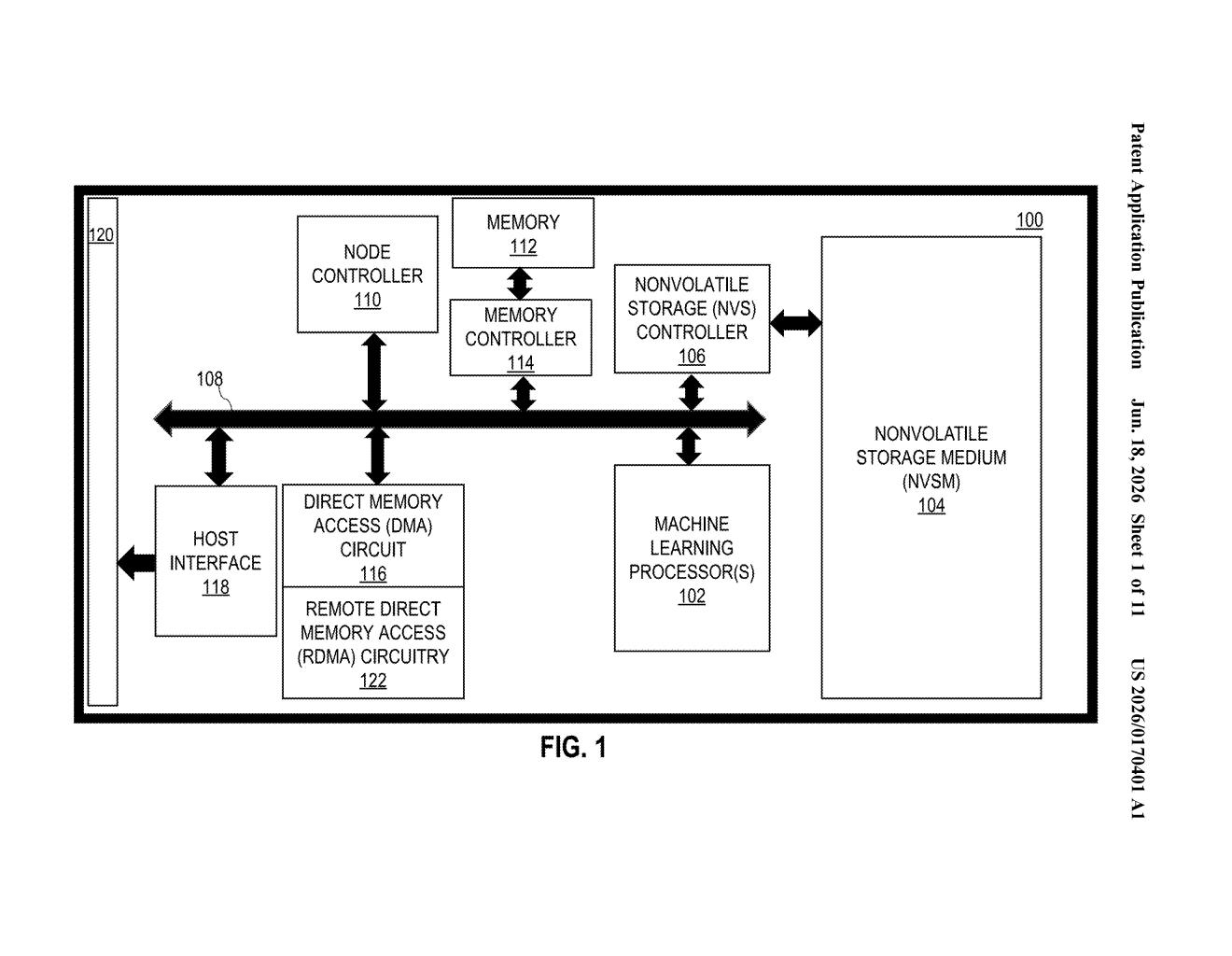
What IBM's compute-inside-storage idea actually does
Imagine your kitchen has a fridge that not only stores ingredients but also chops and cooks them itself, without you having to carry everything to the stove first. IBM's patent describes something like that for computers.
Right now, when an AI system needs to crunch through a huge pile of data, it has to shuttle that data from storage over to the main processor. That back-and-forth takes time and energy. IBM's idea is to put dedicated AI chips directly inside the storage unit, so the crunching happens right where the data already lives.
A small built-in controller manages those AI chips and takes instructions from the main computer. The main processor tells the storage node what to do — but doesn't have to do the actual AI work itself. It's a division of labor meant to speed things up and reduce the traffic between storage and processor.
How the node controller manages the AI processors
The patent describes a machine learning storage node — a self-contained unit that pairs nonvolatile storage (think flash memory or SSDs, storage that keeps data even when the power is off) with one or more dedicated AI processors, all wired together on a shared internal communication bus.
A node controller sits at the center of the unit. It receives high-level commands from the host processor (the main CPU or server chip running the overall system) and translates those into instructions for the AI processors inside the node. The AI processors then pull data directly from the built-in storage and run their machine learning operations locally — no need to send raw data across the system to a separate chip.
Key components of the node:
- Node controller — the traffic cop that interprets commands from the host and manages the AI chips
- Nonvolatile storage medium — the flash or SSD layer that holds the training data or model weights
- ML processors — chips dedicated exclusively to AI math (matrix multiplications, vector operations, etc.)
- Communication bus — the internal link tying all three components together
The key design choice is that the host processor stays in charge of orchestration, but offloads the actual computation to the node — keeping the main CPU free for other tasks.
What this means for data center AI workloads
Moving AI computation closer to stored data is a well-known goal in the industry, often called near-data processing. The core problem it solves is bandwidth: shuttling massive datasets from storage to a remote GPU or CPU is slow and power-hungry. If the AI work happens inside the storage unit, that bottleneck shrinks considerably.
For large-scale data centers running continuous AI inference or training jobs, this architecture could mean more work done per watt and lower pressure on the central processors. IBM is a major player in enterprise server and storage hardware, so this patent fits a strategy of differentiating its storage products with on-device intelligence rather than relying entirely on attached GPU farms.
This is a solid infrastructure patent rather than a flashy consumer-facing idea, but the underlying problem it targets — the cost of moving data to computation — is real and increasingly painful as AI workloads scale. IBM has been here before with in-storage processing concepts, so this looks like continued iteration on a genuine engineering direction, not a one-off filing. Worth watching if you follow enterprise AI infrastructure.
Get one Big Tech patent every Sunday
Plain English, intelligent commentary, no hype. Free.
Editorial commentary on a publicly published patent application. Not legal advice.