
Nvidia Patents Technology to Stop Circuit Components From Crowding Each Other on Silicon
Nvidia is borrowing a technique normally used to render video game graphics and turning it into a tool for designing chips. The idea: use a GPU's built-in shape-tracking ability to instantly spot where circuit components are illegally stacked on top of each other.
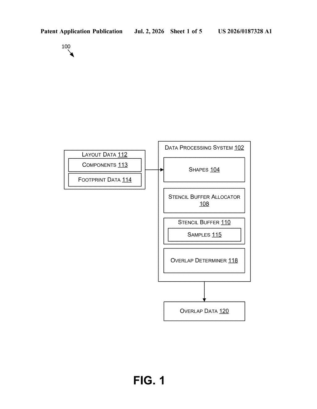
How Nvidia borrows a graphics trick for chip design
Imagine trying to arrange hundreds of furniture pieces in a floor plan, but some overlap each other and that breaks the rules. You need a fast way to find every overlap so you can move things around until nothing is touching.
Nvidia's patent applies the same logic to circuit layout design, where thousands of geometric shapes have to fit on a chip without overlapping. The system uses a graphics technique called a stencil buffer (the same kind your GPU uses when drawing transparent glass in a video game) to count exactly how many shapes land on each tiny point of the layout.
When the count at any point goes above one, there's an overlap, and the system flags it. A generative design tool can then use those flags to automatically nudge shapes into legal positions. It's essentially giving an AI chip-designer a real-time collision sensor.
How the stencil buffer counts overlapping shapes per pixel
The patent describes a system where a processor, likely a GPU, takes a complete set of 2D shapes that make up a circuit layout and renders them into a stencil buffer (a low-level graphics memory structure that records how many shapes cover each pixel-like sample point in an image).
For every point in the image, the stencil buffer holds a count: zero shapes, one shape, two shapes, and so on. Any point with a count greater than one signals an overlap, which in chip design is a physical rule violation where two wires or components occupy the same space.
- The system identifies all shapes in the layout.
- It allocates a stencil buffer mapped to the image dimensions.
- It renders the shapes into the buffer, incrementing the count per point per shape.
- It reads the overlap counts and uses them to guide repositioning of shapes.
The clever part is that GPUs are already highly optimized for exactly this kind of per-pixel counting during normal graphics rendering, so the approach offloads a traditionally slow design-rule check onto hardware that handles it very fast. The output feeds into a generative layout tool, an AI system that iterates on placements until all overlaps are resolved.
What this means for AI-generated circuit layouts
Chip design is one of the most expensive and time-consuming processes in the semiconductor industry, and a big part of that cost comes from verifying that shapes in a layout don't violate physical rules. Traditionally this is done with specialized software that checks rules one by one. Using GPU stencil buffers to count overlaps turns a slow sequential check into a massively parallel graphics operation, which could dramatically speed up each iteration in an AI-driven layout loop.
For Nvidia, which sells both the GPUs used for AI workloads and the cuLitho computational lithography software, this kind of technique fits a broader push to use its own hardware to accelerate chip manufacturing workflows. Faster overlap detection means a generative AI can try more layout configurations in the same time, potentially producing better chip designs.
This is a genuinely clever piece of cross-domain engineering: taking a graphics primitive that's been in GPUs for decades and repurposing it for electronic design automation. It's not flashy, but it's the kind of low-level optimization that compounds into real speed gains when you're running millions of layout iterations. Worth watching as a signal of how Nvidia is weaving its GPU capabilities into the chip-design pipeline itself.
Get our take in your Top Stories
Liked this breakdown? Add Patentlyze as a preferred source on Google, and our plain-English take shows up more often in your Top Stories the next time Nvidia patent news breaks.
There are more where this came from
We read every patent application Big Tech publishes and send you the ones worth knowing. Plain English, free, every week.
Want this weekly breakdown for a company we don't cover? Patentlyze Pro →