
Samsung Patents a Faster Way to Test Memory Chip Connections Before Building Them
Before a memory chip ever gets soldered onto a circuit board, engineers have to simulate thousands of electrical interactions to make sure nothing will fail. Samsung has filed a patent for a method that makes those simulations faster and more manageable by splitting up the problem in a clever way.
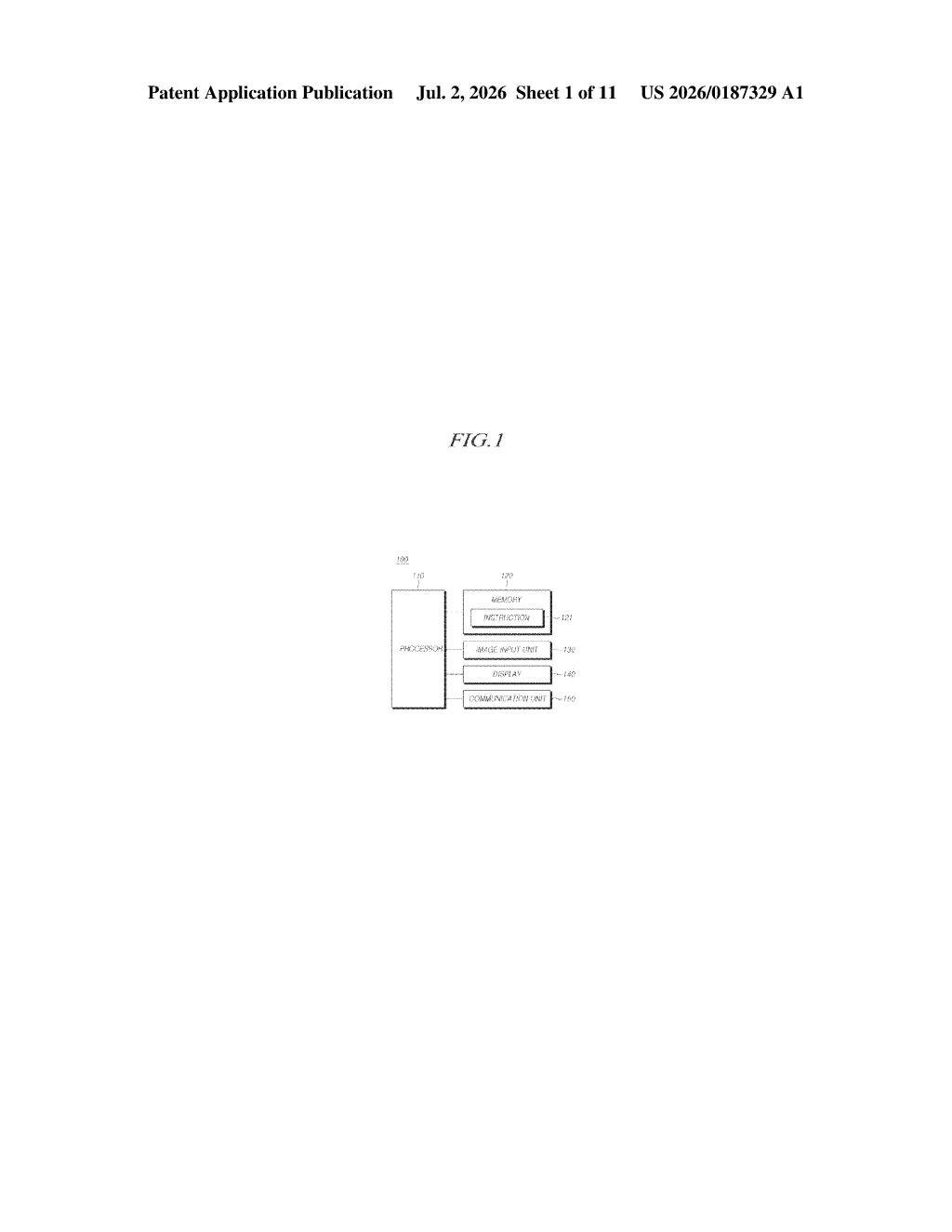
What Samsung's memory simulation shortcut actually does
Imagine you're an architect who needs to check whether every pipe, wire, and load-bearing wall in a skyscraper will hold up before you break ground. Running one giant check on everything at once is slow and unwieldy. Instead, you split the building into zones and test each one separately. That's essentially what Samsung is doing here, but for memory chips.
When Samsung designs a chip that reads and writes data quickly (like the memory inside a phone or a server), engineers simulate how electrical signals travel between components before any hardware is built. The problem is that these simulations bundle together a lot of complex models, making them slow and hard to debug.
Samsung's patent describes a method that separates the simulation into distinct pieces, including the signal path, the power delivery network, and the logic circuit, then tests each piece with a simplified stand-in current source. The result is a simulation that is easier to run, easier to understand, and faster to complete.
How Samsung separates the circuit models to speed up simulation
The patent describes a simulation method for memory interfaces, the electrical connections that let a processor talk to RAM chips at high speed.
The core steps are:
- Separate the models: The method splits apart two standard simulation tools: a channel model (which describes how a signal travels along a wire or trace on a circuit board) and an IBIS model (Input/Output Buffer Information Specification, essentially a standardized description of how a chip's pins behave electrically).
- Short the transmitting terminal: By temporarily connecting the output pin of the IBIS model directly to ground, engineers can isolate and extract a current profile, a snapshot of how much current the entire logic circuit draws over time.
- Identify and model the subsystems: The simulation then separately characterizes the logic circuit, the power delivery network (PDN, the system of capacitors and traces that keep voltage steady), and the signal path.
- Apply a temporary current source: Instead of running the full, complex IBIS model every time, the method substitutes a simplified current source into the PDN simulation. This acts as a stand-in that reproduces the electrical behavior without the computational overhead.
The net effect is a modular simulation workflow that is easier to validate and faster to iterate on during chip development.
What this means for Samsung's chip design pipeline
Memory interface reliability is a make-or-break issue in chip design. If the power delivery network droops or a signal arrives distorted, a chip can crash or produce errors, and finding that out after manufacturing is expensive. Simulation tools that can catch these problems earlier and faster directly reduce development cost and time.
For Samsung, which designs both the memory chips (like LPDDR and HBM) and the processors that use them, having tighter control over simulation methodology is a practical engineering advantage. This patent is squarely in the territory of internal design tooling, so it is unlikely to show up in a product announcement, but it reflects the kind of incremental process work that adds up to faster, more reliable chip releases.
This is a narrow, process-oriented patent aimed squarely at Samsung's own chip engineering teams. It is not the kind of filing that signals a new product direction or a big strategic bet. If you work in EDA (electronic design automation) or memory chip development, the modular simulation approach is genuinely useful. For everyone else, this is routine infrastructure work.
Get our take in your Top Stories
Liked this breakdown? Add Patentlyze as a preferred source on Google, and our plain-English take shows up more often in your Top Stories the next time Samsung patent news breaks.
There are more where this came from
We read every patent application Big Tech publishes and send you the ones worth knowing. Plain English, free, every week.
Want this weekly breakdown for a company we don't cover? Patentlyze Pro →