
Samsung Display Patents a Screen Layer Design That Tunes Each Color Separately
Getting red, green, and blue light to all look equally bright and sharp on the same OLED panel is harder than it sounds. Samsung Display is patenting a way to give each color its own custom electrode structure, built into the pixel itself.
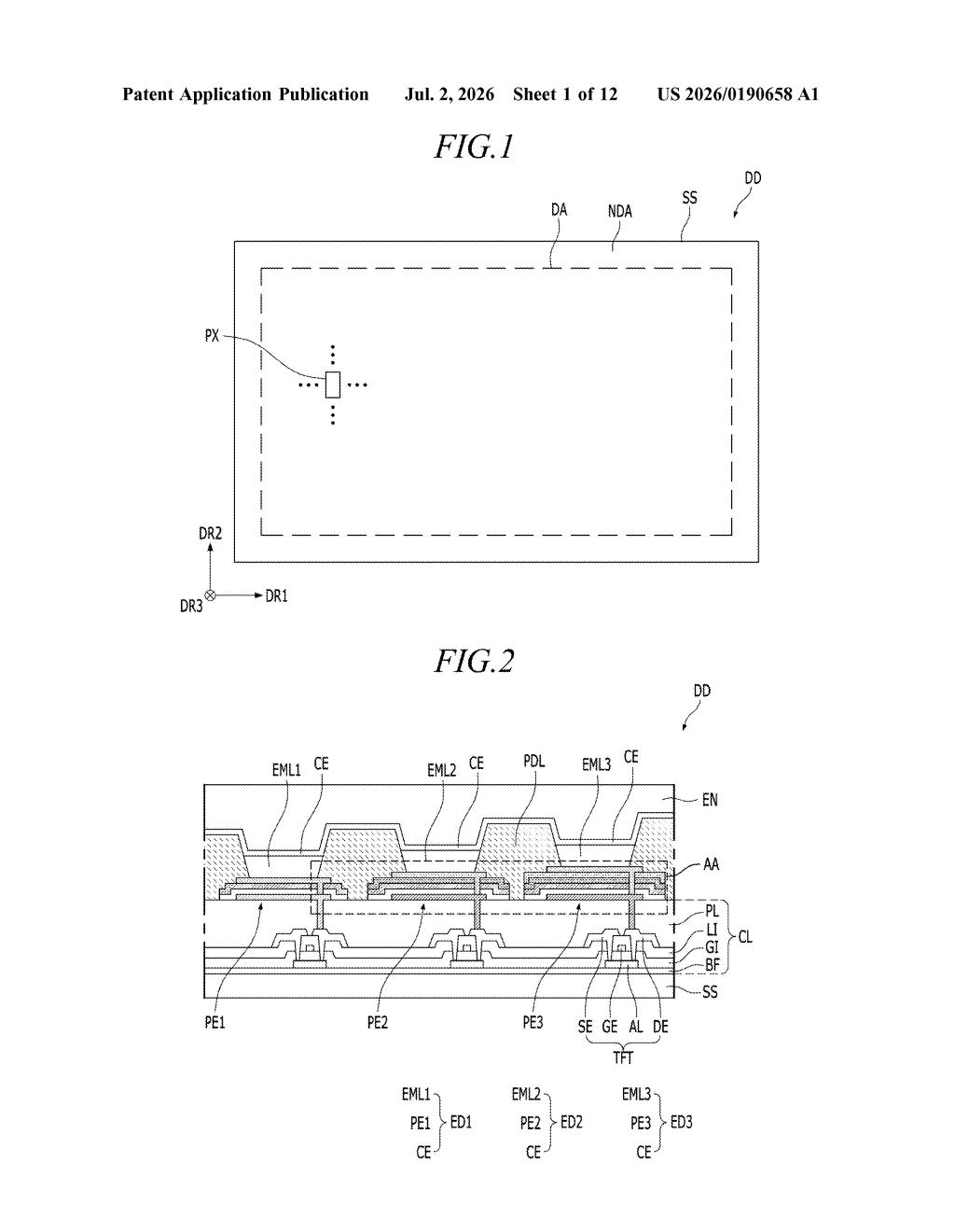
What Samsung's different-thickness pixel stack actually does
Imagine you're mixing paint: red, green, and blue pigments don't behave the same way, so you'd adjust each one differently to get a balanced result. OLED screens face a similar problem. Each tiny pixel has to produce exactly the right amount of light, and the electrode layers that drive those pixels need to be tuned for each color.
Samsung Display's patent describes a display where the electrodes underneath different colored pixels are built up with a different number of layers, making them physically thicker or thinner depending on which color they serve. One pixel type gets four layers stacked in a specific order; another gets five. Both share a common top electrode.
The clever part is that one particular layer, called the inorganic layer, is kept at the same thickness in both pixel types. That keeps the manufacturing process consistent while still allowing the overall electrode height to differ. It's a way of fine-tuning optical performance without requiring a completely different fabrication line for each color.
How the inorganic and hard-mask layers are stacked per pixel
The patent covers an OLED display structure built on a substrate, where two types of light-emitting diodes sit side by side. Each diode has its own pixel electrode (the bottom conductor that drives light out of the organic material above it) and shares a single common electrode on top.
The first pixel electrode is built from four layers in order: a lower metal layer, an inorganic layer (a non-metallic material like silicon nitride or oxide), a hard mask layer (used during manufacturing to protect parts of the stack during etching), and an upper metal layer.
The second pixel electrode adds one extra layer: it goes lower metal, inorganic, hard mask, a third inorganic layer, then upper metal. That extra inorganic layer is what makes the second electrode physically taller.
- Both electrodes have contact holes drilled through their middle layers so electrical signals can reach the transistors below.
- The first inorganic layer and second inorganic layer are kept at the same thickness, which matters for process control during manufacturing.
- The total thickness of each electrode differs because of the extra layer in the second type, and that thickness difference changes how light bounces inside the pixel cavity, affecting which wavelength (color) comes out most efficiently.
What this means for next-generation OLED screen quality
OLED panels rely on a phenomenon called optical microcavity: the distance between the bottom and top electrodes acts like a tiny resonator that amplifies certain wavelengths. If red, green, and blue pixels all had identical electrode stacks, one or two colors would inevitably be dimmer or less pure than the others. Tuning electrode thickness per color is a known engineering approach, and this patent describes a specific way to do it while keeping part of the stack uniform across all pixels.
For consumers, the downstream effect is a screen that can hit more accurate colors and better brightness balance without the manufacturer having to run a separate deposition step for each color channel. Whether this specific architecture ends up in Samsung's Galaxy phones, tablets, or TV panels isn't clear from the filing alone, but it fits squarely in the company's ongoing work on high-efficiency OLED displays.
This is deep manufacturing-process IP, not a product feature you'll ever see advertised on a spec sheet. It's the kind of incremental structural patent that display makers file constantly to protect fabrication know-how. It matters to Samsung's competitive position in OLED manufacturing, but it won't change how anyone thinks about buying a phone.
Get our take in your Top Stories
Liked this breakdown? Add Patentlyze as a preferred source on Google, and our plain-English take shows up more often in your Top Stories the next time Samsung patent news breaks.
There are more where this came from
We read every patent application Big Tech publishes and send you the ones worth knowing. Plain English, free, every week.
Want this weekly breakdown for a company we don't cover? Patentlyze Pro →