
Samsung's New Patent Tries to Shrink the Black Border Around Phone Screens
Samsung Display has filed a patent describing a new way to arrange the internal wiring strips that sit at the edge of a phone screen, and the goal appears to be squeezing those components into a tighter space so the visible border around the display can shrink.
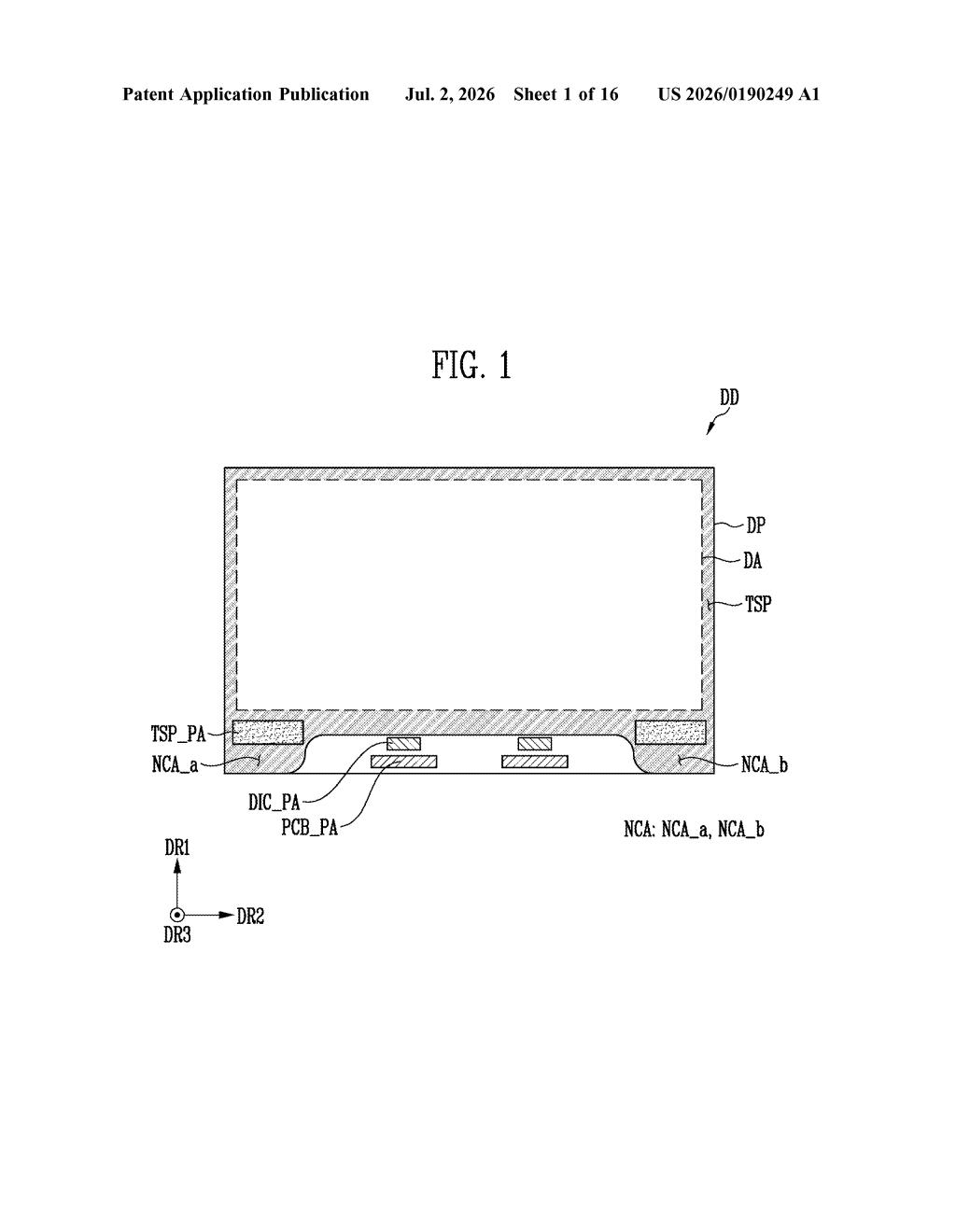
What Samsung's border-shrinking display layout actually does
Picture the thin black strip that runs around the edge of your phone screen. Inside that strip, behind the glass, there are flexible circuit boards that carry signals to and from the display. The thinner engineers can make that strip, the more screen you get in the same size device.
Samsung's patent describes a specific geometric trick: the non-display area of the screen panel grows small finger-like extensions that poke outward, and the circuit board is shaped to nestle right alongside those extensions rather than sitting completely beneath them. Think of it like puzzle pieces fitting next to each other instead of stacking on top.
The design also involves a touch sensor with a notch cut into it, positioned so it doesn't overlap the wiring connectors at the panel's edge. Together, these shapes are meant to reduce wasted space and potentially let the border around your screen get a little narrower.
How the protrusion-and-PCB geometry fits together
The patent covers the physical geometry of three layers stacked inside a display assembly: the display panel itself, a touch sensor layer on top of it, and a polarizing (anti-glare) layer on top of that. A flexible printed circuit board (a thin ribbon of wiring) connects at the edge.
The key claim is about the non-display area, the inactive region around the screen's perimeter. Samsung's design gives this border one or more protrusions, small rectangular tabs that extend outward from the active screen area toward the connector pads. The circuit board is then shaped so its own tabs extend in the opposite direction, sliding alongside those protrusions rather than overlapping them vertically.
The touch sensor has a notch cut out of it that runs in the same direction as these protrusions but is positioned so it avoids sitting directly on top of the electrical pads. This matters because having multiple thick layers stacked directly over a connector pad can interfere with the bond and add unwanted height.
By interleaving these shapes side by side (rather than stacking everything on top of each other), the overall border footprint can in theory be reduced without sacrificing the number of electrical connections the panel needs.
What this means for phone and tablet bezels
Bezel size is one of the most visible ways phone and tablet makers compete, and shaving even a fraction of a millimeter off the border is a genuine engineering challenge at this scale. A new arrangement of how circuit boards connect to a display panel is the kind of incremental, unglamorous work that actually moves that needle over time. If Samsung Display ships this approach, you could see it in future Galaxy phones or foldables where thin borders are especially important.
It's also worth noting that Samsung Display supplies screens to many device makers beyond Samsung's own phone division, so any manufacturing change here could ripple into products from other brands too. That said, this is an early-stage filing and there's a long road between a patent and a finished product on a store shelf.
This is quiet display-engineering work, not a headline product feature. It's the kind of patent that matters to manufacturing teams trying to hit a bezel specification rather than to consumers picking a phone. Worth tracking if you follow display supply-chain news, but not something that signals a dramatic new direction for Samsung.
Get our take in your Top Stories
Liked this breakdown? Add Patentlyze as a preferred source on Google, and our plain-English take shows up more often in your Top Stories the next time Samsung patent news breaks.
There are more where this came from
We read every patent application Big Tech publishes and send you the ones worth knowing. Plain English, free, every week.
Want this weekly breakdown for a company we don't cover? Patentlyze Pro →