
Sony Patent Filing Targets Noise Reduction in Stacked Three-Chip Camera Sensors
Most camera sensors are one flat chip doing everything at once. Sony's new patent describes splitting that job across three separate chips bonded together, each handling a different part of turning light into a clean image.
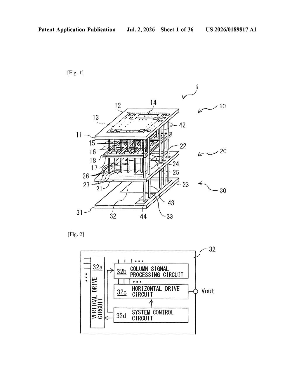
What Sony's three-layer image sensor actually does
Imagine your camera sensor as a tiny factory. Right now, one floor handles everything: collecting light, reading the signal, and deciding what to do with it. Sony's patent describes splitting that factory into three specialized floors stacked on top of each other, each doing one job well.
The top layer collects light. A middle layer handles reading out the electrical signals those photons create. A bottom layer runs the logic that controls the whole operation and compares signals to reduce noise. One of the key moves here is a reference-voltage wire that runs between adjacent pixel regions to act as a kind of electrical ground truth, helping the system identify and subtract out unwanted noise.
The three layers are bonded together physically and connected by tiny vertical wires called through-silicon vias, which act like elevator shafts for electrical signals. The result is a sensor where the light-collection layer stays clean and simple, while more complex processing happens below it.
How the stacked chip layers talk to each other
The patent describes a three-section stacked semiconductor device aimed at image sensors. Each section is a separate chip (semiconductor substrate), and they are bonded face-to-face in a vertical stack.
- First section (top): Contains the pixel array, meaning the photoelectric conversion regions that turn incoming photons into electrical charge. Each pixel has a floating diffusion node (a tiny charge-storage area) and bonding pads that connect downward.
- Second section (middle): Contains the readout circuitry that picks up the charge signals from the top layer through those bonding pads.
- Third section (bottom): Houses the logic circuit that controls the array and, critically, processes the signals it receives.
The logic layer collects two distinct signals from the pixel array: a first signal (a reference or baseline read) and a second signal (the actual image data). It then generates a third signal by subtracting or comparing the two. This is a technique called correlated double sampling, which removes fixed-pattern noise that would otherwise degrade image quality.
Vertical connectivity across all three layers is handled by through-silicon vias (TSVs), which are microscopic conductive columns drilled through the silicon. A dedicated reference-voltage wiring line also runs between adjacent pixel columns in the top layer to stabilize electrical potential and reduce interference between neighboring pixels.
What this means for future Sony camera sensors
Stacking sensor layers is not new, Sony's own back-illuminated and stacked CMOS sensors already use a two-chip approach. What this patent adds is a three-layer architecture where logic, readout, and light-collection each get dedicated silicon. That separation lets each layer be optimized independently, and it creates more room for the processing circuitry that cleans up the image before it ever leaves the sensor chip.
For you as a camera user, this kind of design can translate to cleaner images in low light, faster readout speeds (which reduce the rolling-shutter distortion you sometimes see when photographing fast motion), and potentially lower power draw. Sony supplies image sensors to a wide range of phone and camera makers, so architecture improvements at the chip level tend to ripple outward into a lot of consumer devices over time.
This is a dense, component-level patent that won't make headlines the way a new iPhone does, but Sony's image sensor division supplies chips to a huge chunk of the camera industry. A three-layer stacked design with on-chip noise reduction built into the logic layer is the kind of foundational work that improves every camera it eventually ends up inside. Worth watching as a signal of where Sony's sensor roadmap is heading.
Get our take in your Top Stories
Liked this breakdown? Add Patentlyze as a preferred source on Google, and our plain-English take shows up more often in your Top Stories the next time Sony patent news breaks.
There are more where this came from
We read every patent application Big Tech publishes and send you the ones worth knowing. Plain English, free, every week.
Want this weekly breakdown for a company we don't cover? Patentlyze Pro →