
Sony Patents a Lighting System That Fills Dark Gaps in Depth-Sensing Cameras
When a camera tries to measure distance using a grid of tiny lasers, the dark gaps between those lasers can cause blind spots. Sony's new patent describes a lens system designed to close those gaps before they become a problem.
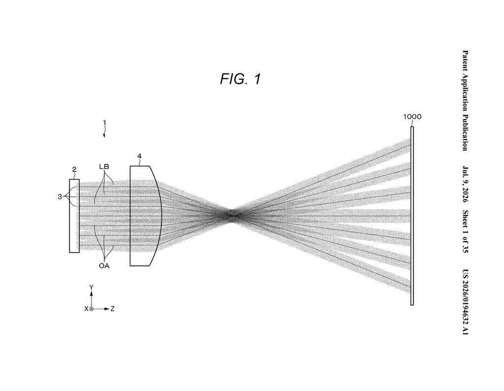
What Sony's gap-filling light array actually does
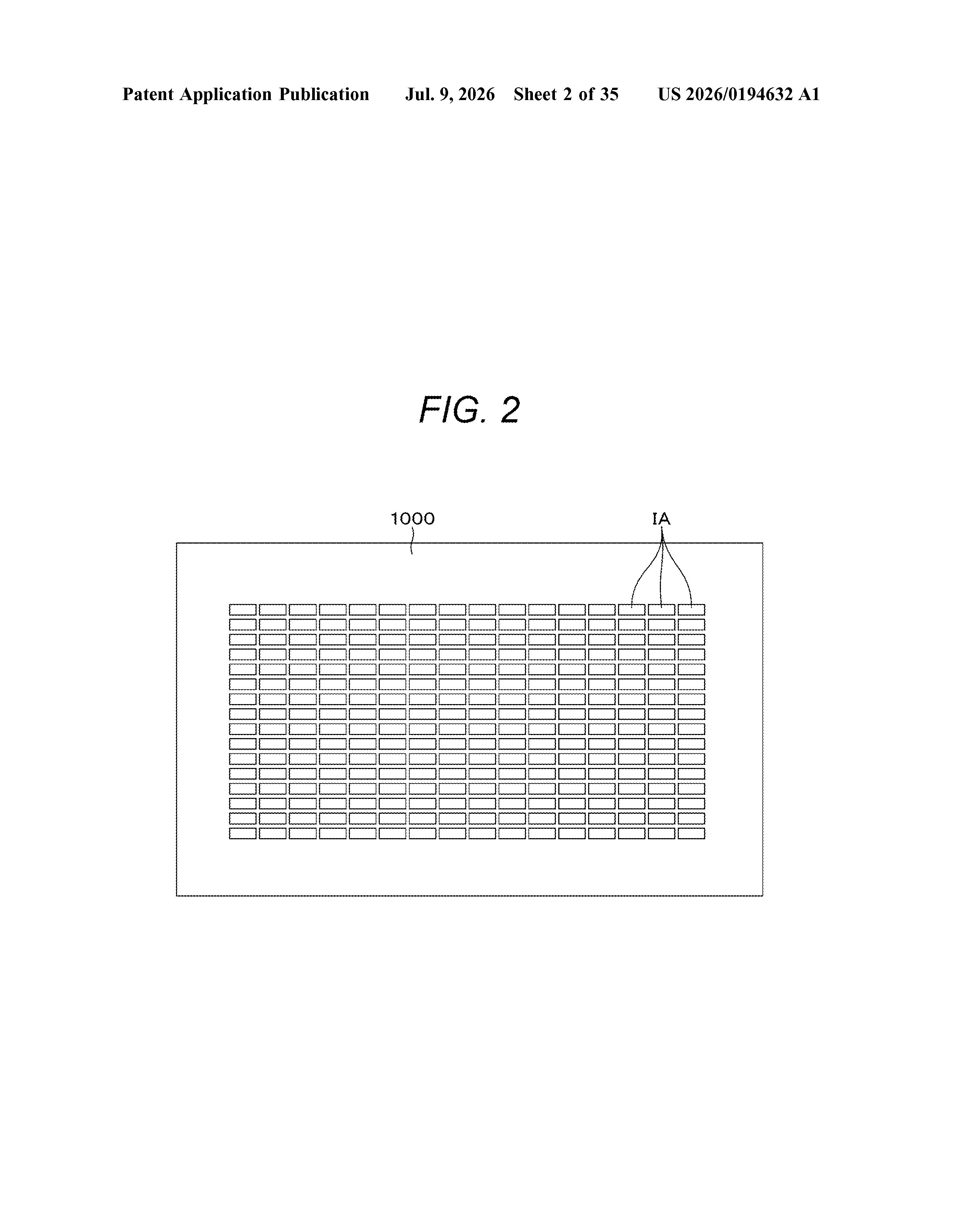
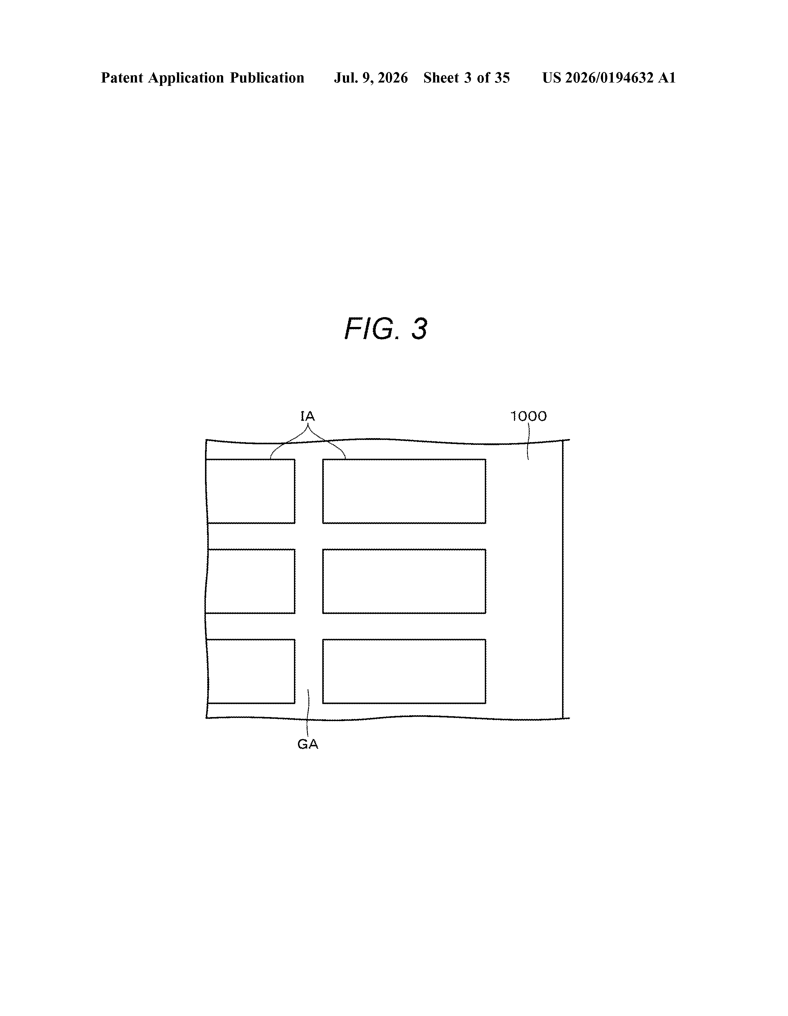
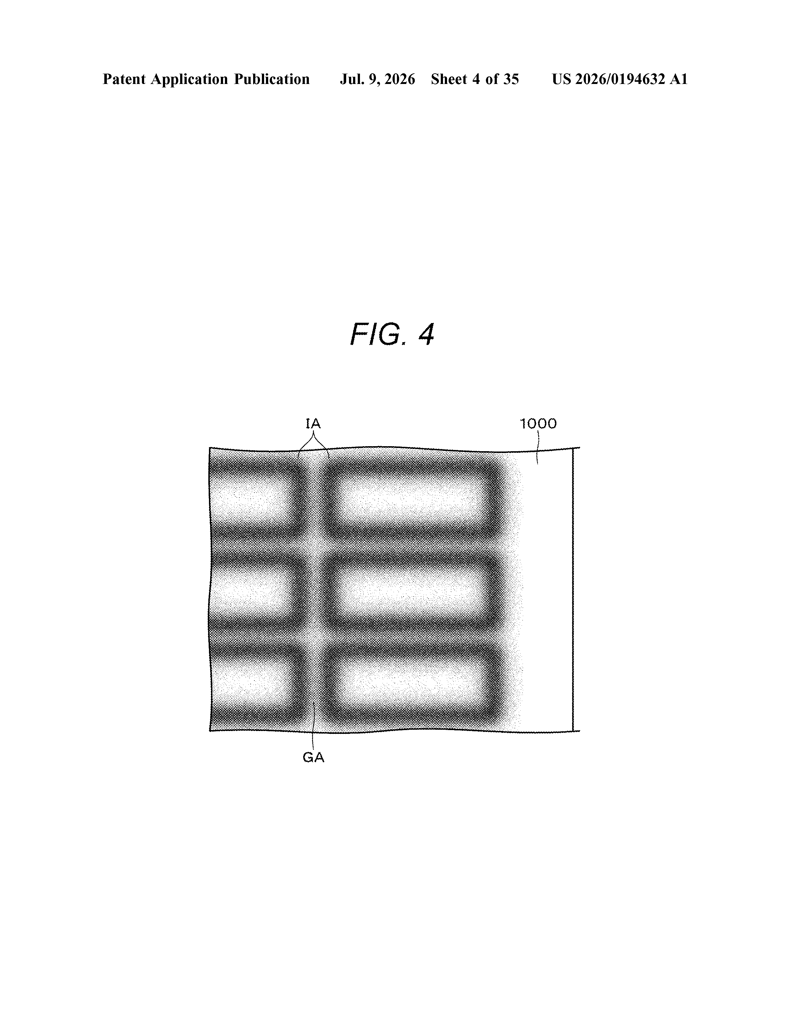
Imagine a flashlight made from dozens of tiny bulbs arranged in a grid. Even if each bulb is bright, there are small dark patches in the spaces between them. Now imagine using that flashlight to measure how far away objects are. Those dark patches mean some parts of the scene get missed entirely.
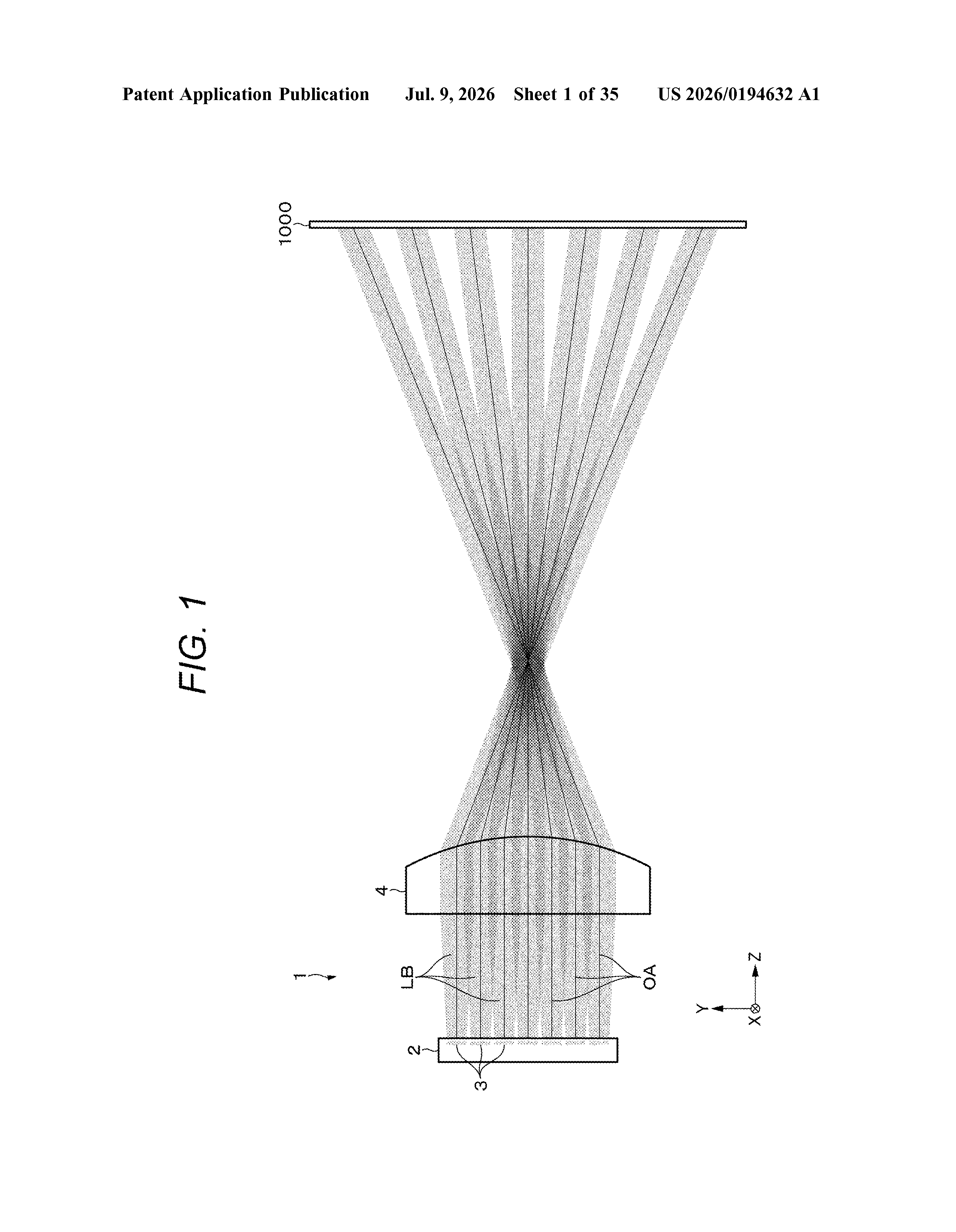
That's exactly the challenge Sony's engineers are tackling here. Their design adds a specially shaped optical layer right in front of the array of light emitters. This layer bends and blends the individual beams so the gaps between them close up, and the brightness evens out across the whole field.
A second lens then takes that now-unified sheet of light and straightens it into a roughly parallel beam aimed at the scene. The result is a more complete, uniform patch of light, which should give a depth sensor far fewer blind spots to deal with.
How the two-lens stack merges and evens the beams
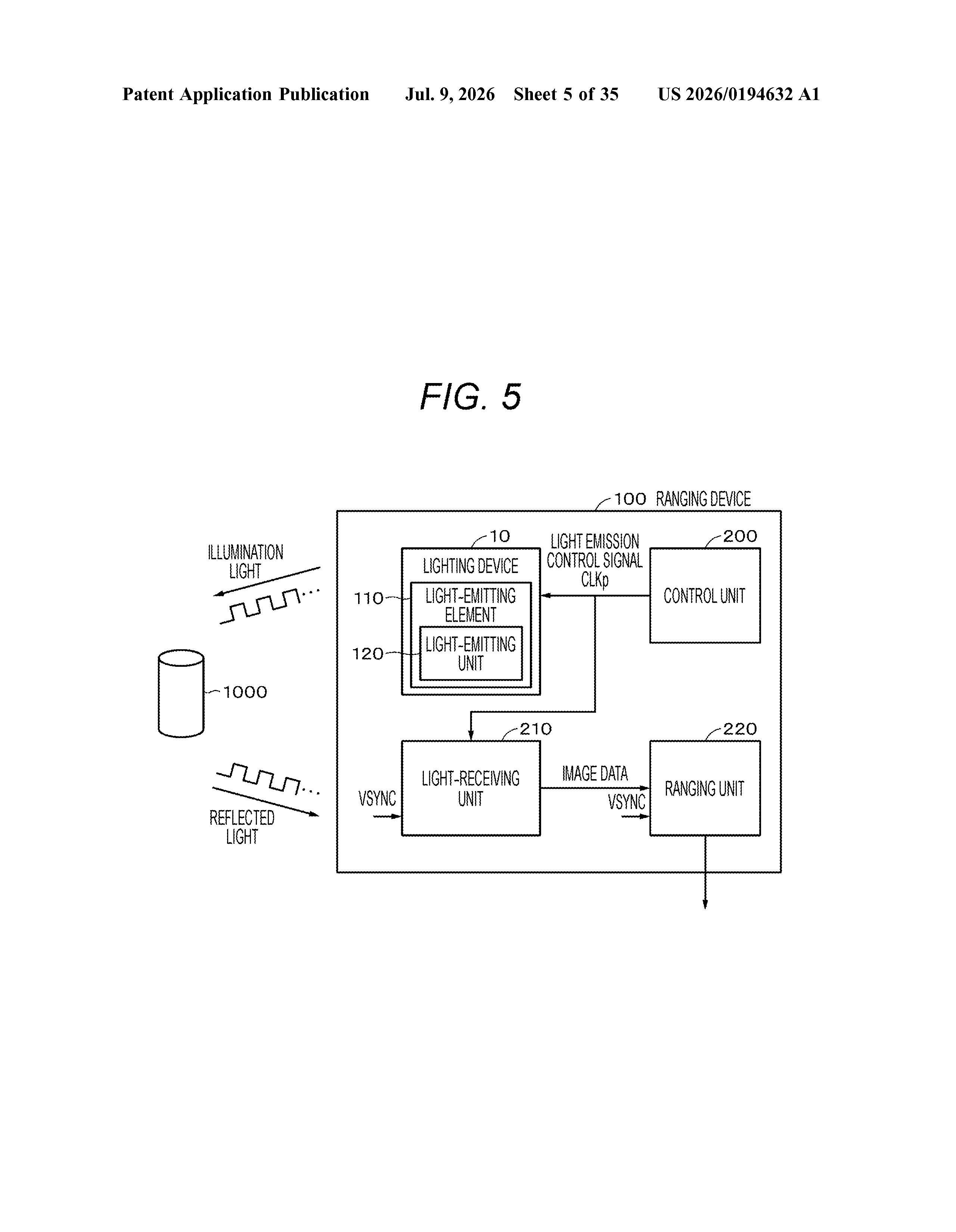
The patent describes a three-part assembly for a lighting module used in ranging devices (hardware that measures the distance to objects, like a LiDAR or time-of-flight sensor).
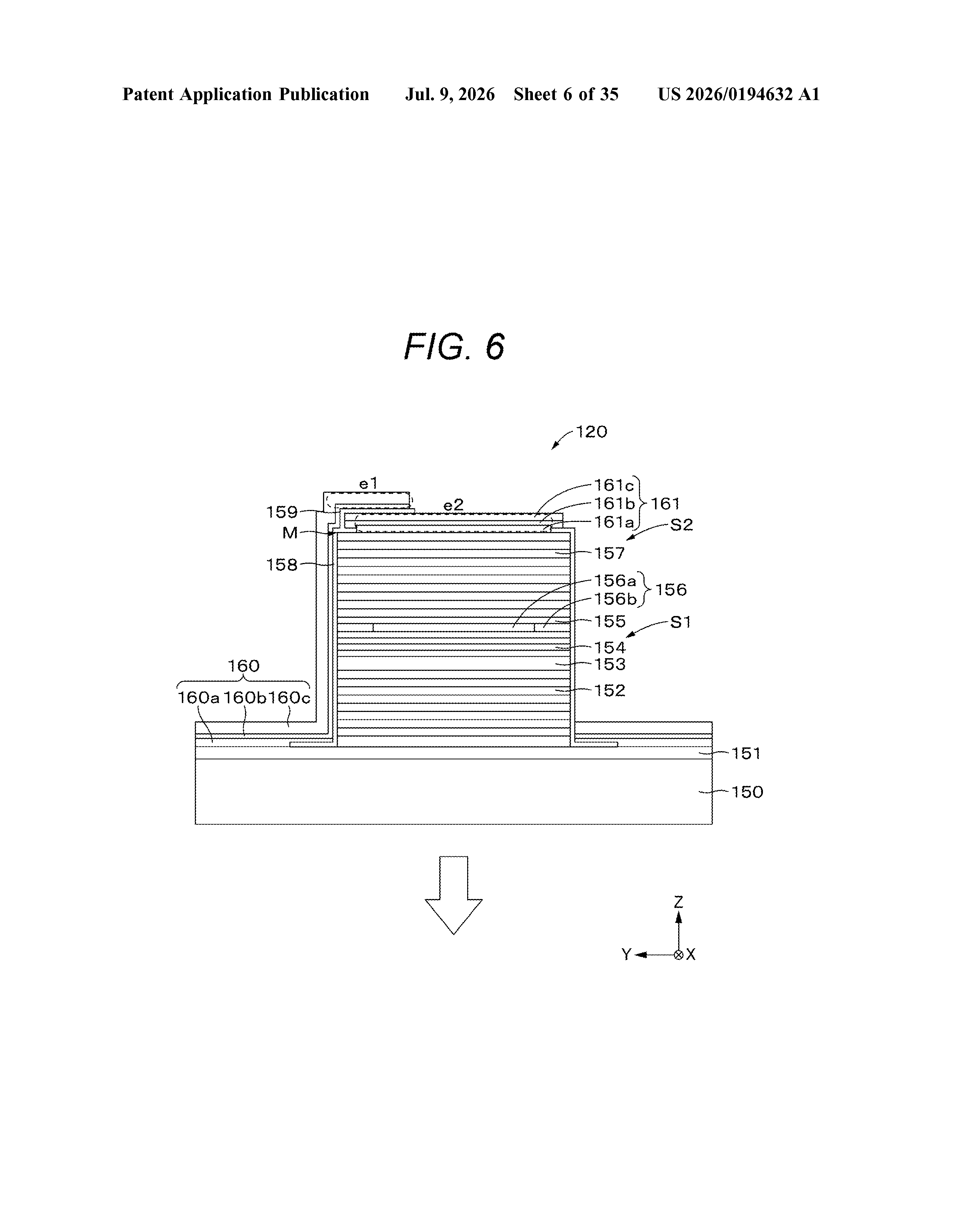
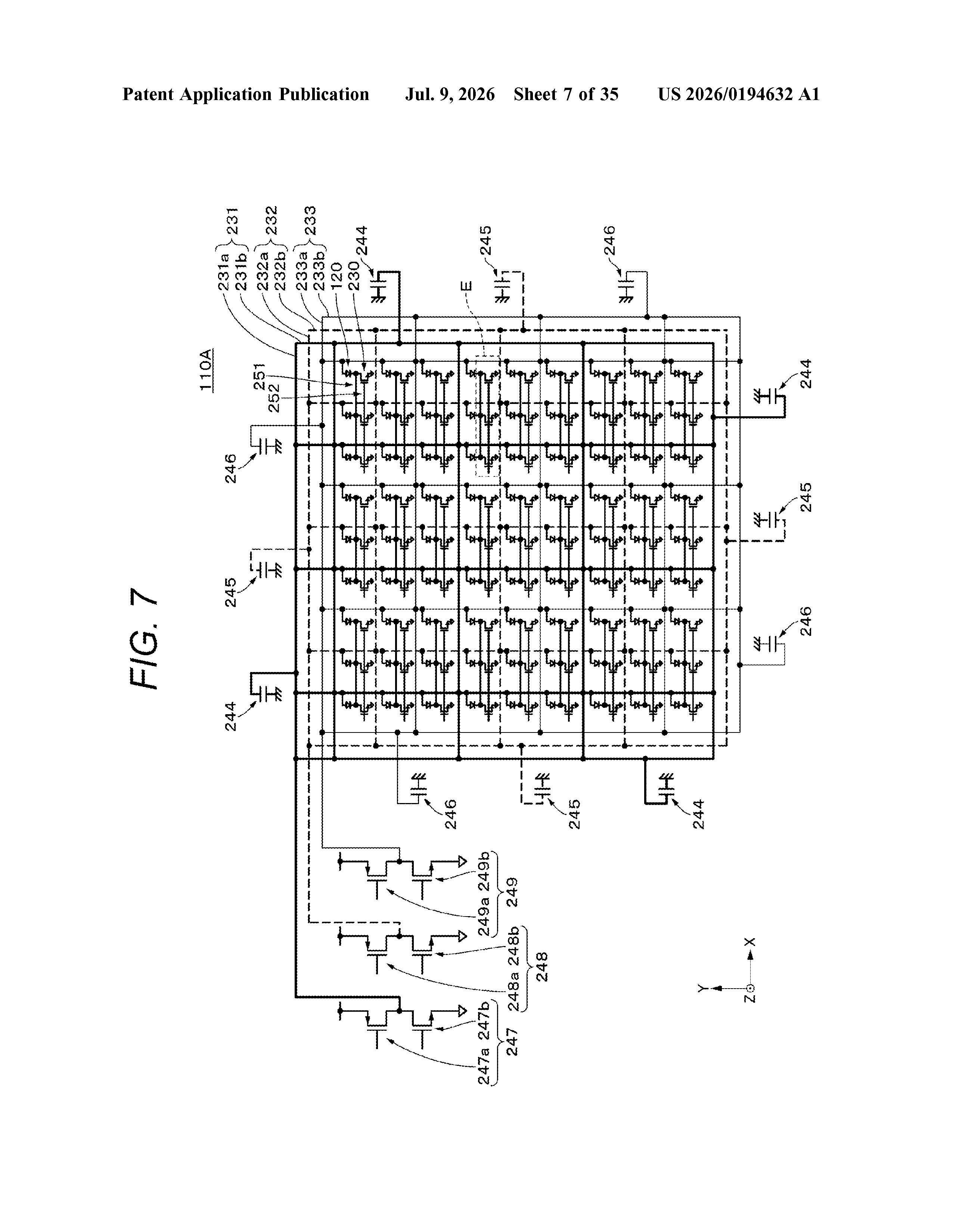
- Light-emitting element: A grid of individual light-emitting units, most likely VCSELs (vertical-cavity surface-emitting lasers, a common type of tiny laser used in face-unlock and depth cameras).
- First optical member: A lens or structured optical element placed very close to the emitter array. Its job is to redirect light from each emitter so the beams overlap at their edges, closing the dark gaps between adjacent emitters and equalizing the brightness across the full array.
- Second optical member: A collimating lens (one that takes spreading light and makes the rays roughly parallel) that shapes the now-uniform output into a directed beam suitable for illuminating a target scene.
The key innovation is that first optical layer doing double duty: reducing gaps and leveling out intensity variation, two problems that normally require separate solutions. The second lens then handles the beam-shaping step downstream.
What this means for 3D sensing in consumer devices
Depth sensors that use arrays of laser emitters are already inside smartphones (for Face ID-style authentication), AR headsets, robotics, and automotive cameras. Any gap in the illumination pattern is a gap in the depth map, which means the sensor can misread edges, miss small objects, or produce patchy 3D reconstructions. A lighting module that addresses this at the optics level, rather than in software, means better raw data from the start.
For Sony Semiconductor Solutions specifically, this is squarely in their core business of selling image sensors and sensing modules to device makers. A more uniform illumination source makes their depth-sensing products more competitive for phone makers, robotics companies, and automotive suppliers who buy Sony components.
This is a focused, practical optics patent with no fluff. It solves a real physics problem that anyone building a LiDAR or time-of-flight module has to deal with. It's not a headline-grabbing AI play, but for Sony's semiconductor customers, uniform illumination is one of those unglamorous details that separates a good depth sensor from a great one.
Get our take in your Top Stories
Liked this breakdown? Add Patentlyze as a preferred source on Google, and our plain-English take shows up more often in your Top Stories the next time Sony patent news breaks.
There are more where this came from
We read every patent application Big Tech publishes and send you the ones worth knowing. Plain English, free, every week.
The drawings
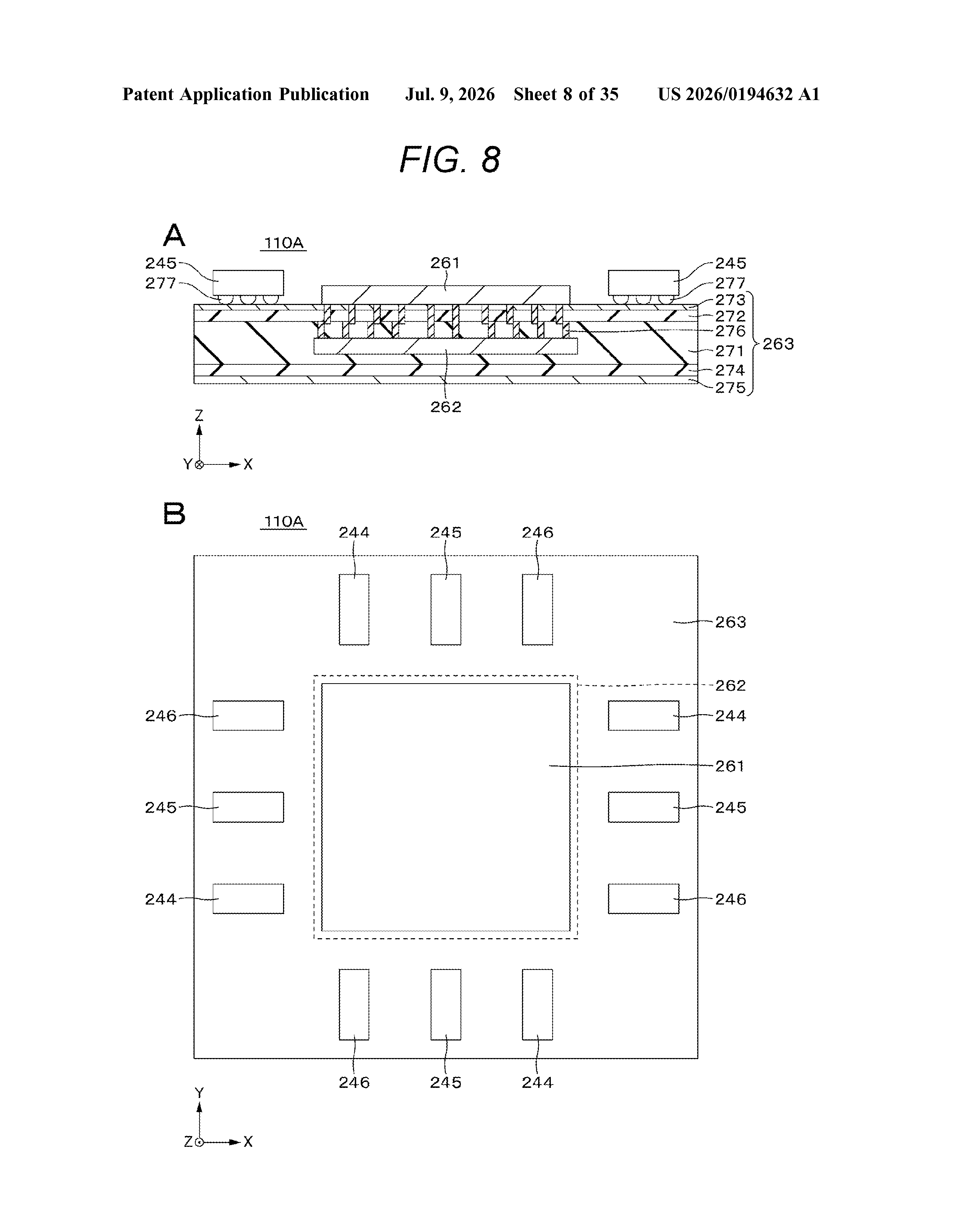
35 drawing sheets from US 2026/0194632 A1 · click any drawing to enlarge
Want this weekly breakdown for a company we don't cover? Patentlyze Pro →