
Samsung Patent Targets Sub-Pixel Layout to Reduce Interference and Sharpen Displays
Every pixel on your phone screen is controlled by a tiny circuit, and Samsung has filed a patent that changes how the wiring inside that circuit is physically arranged. It's a quiet structural tweak, but these kinds of layout decisions directly affect how sharp, bright, and power-efficient a display can be.
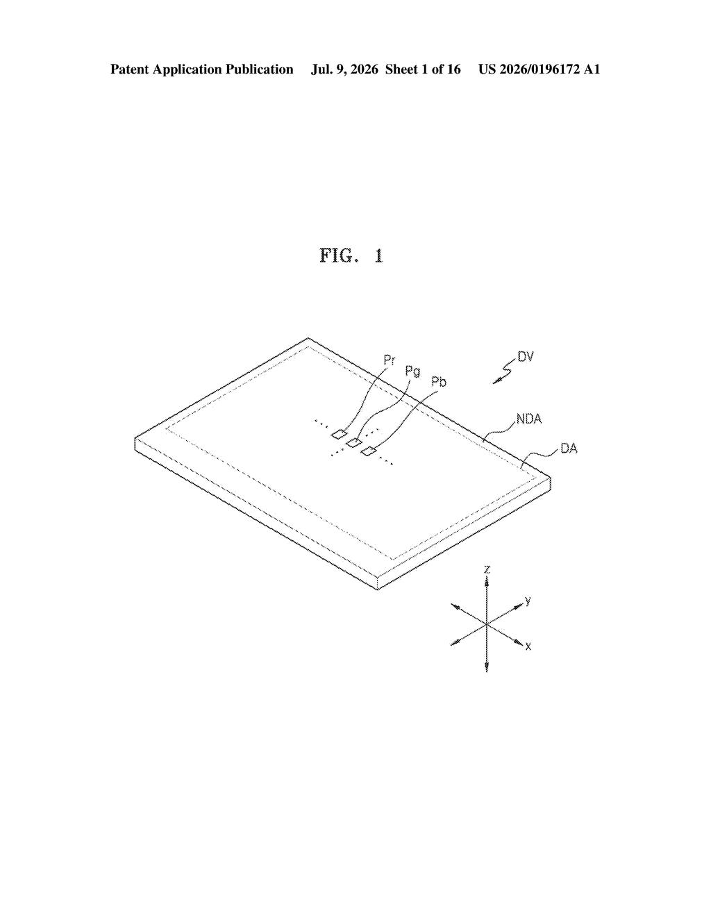
What Samsung's sub-pixel circuit change actually does
Imagine each dot of color on your phone screen as a tiny room with its own light switch and electrical wiring. The way that wiring is laid out inside the room determines how reliably the light turns on, how much space the wiring takes up, and how much electricity it wastes.
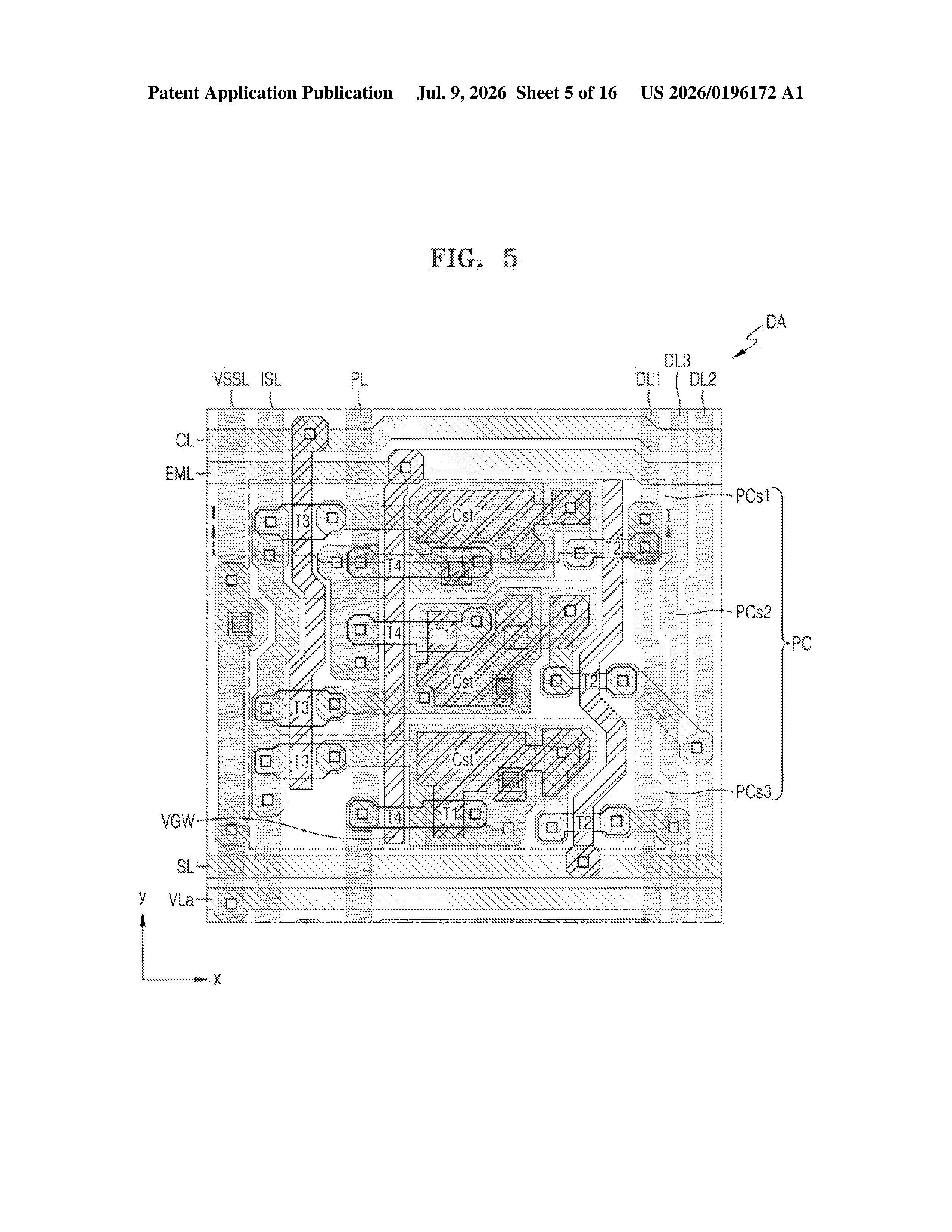
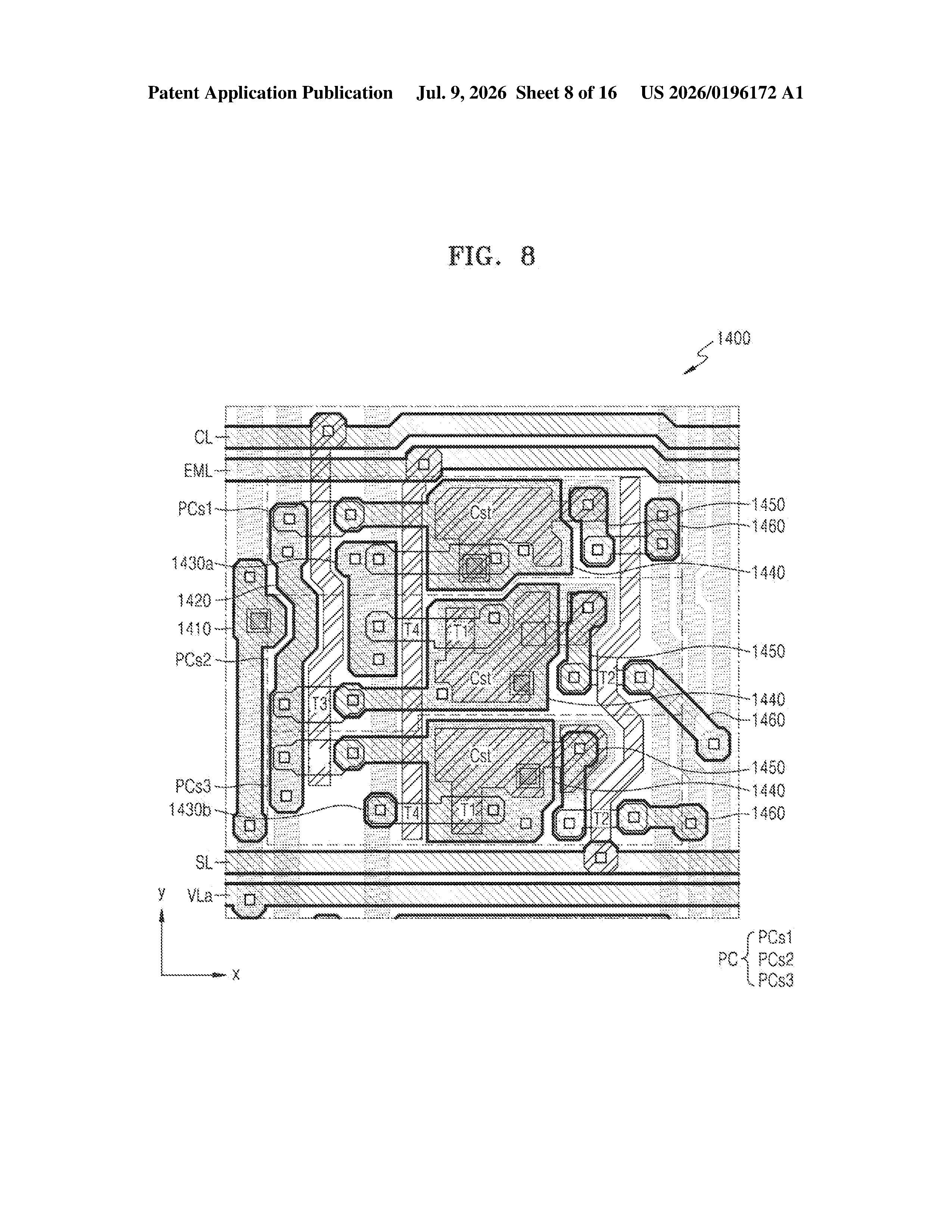
Samsung's patent describes a new floor plan for that room. Specifically, it moves a particular wiring component (called a conductive pattern) to sit physically between the main power line and the transistor that drives the light. That repositioning is meant to make the circuit more orderly and compact.
This is deeply inside-the-factory engineering. You would never notice this change by looking at a finished phone. But display manufacturers obsess over these layouts because small efficiency gains at the pixel level add up across millions of pixels, potentially improving brightness, reducing power draw, or enabling thinner panels.
How Samsung reroutes the emission control path
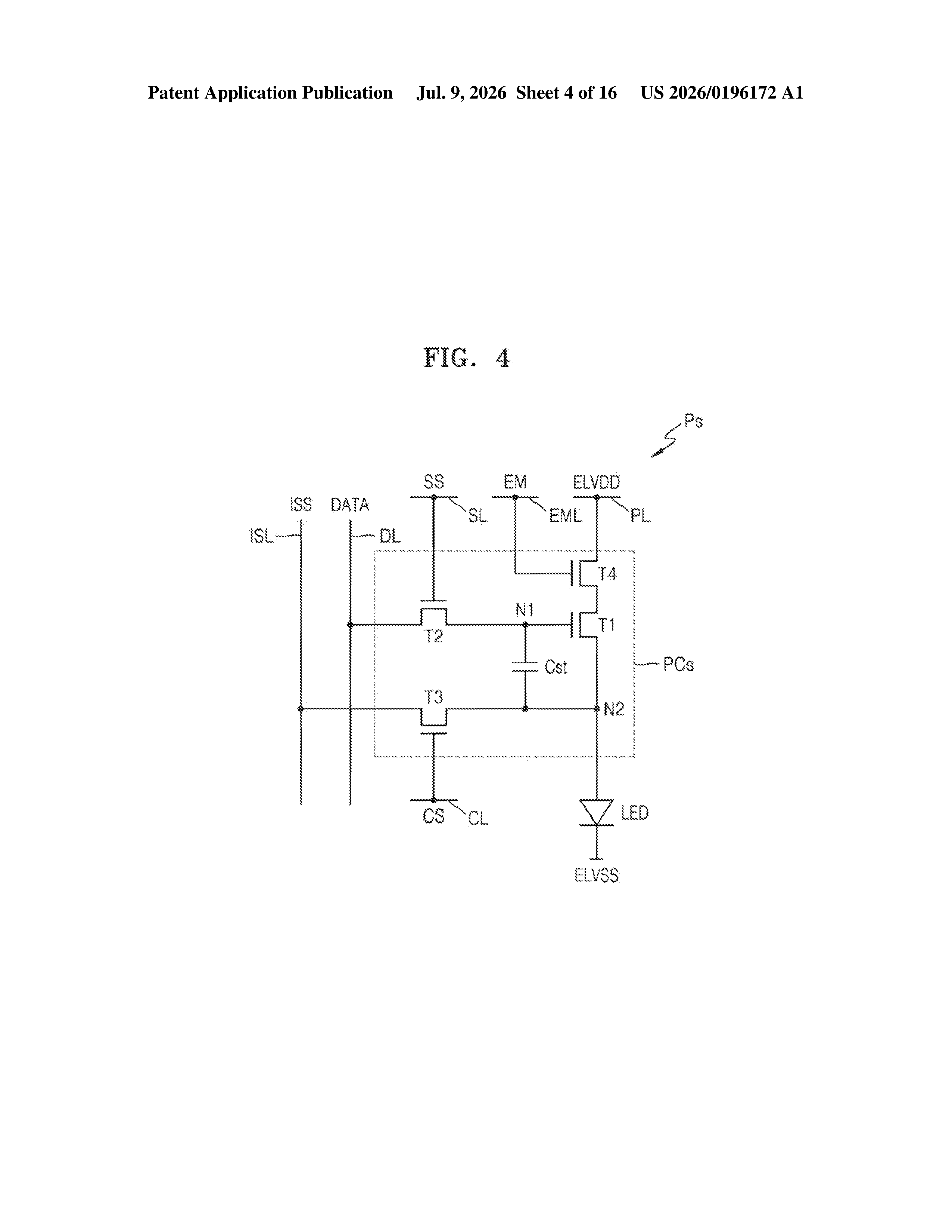
Each pixel in an OLED display is controlled by a small cluster of transistors (tiny electronic switches) that decide when the pixel's light turns on and how bright it should be.
This patent focuses on three of those transistors:
- Driving transistor: controls how much current flows to the light-emitting diode, setting brightness.
- Data write transistor: receives the brightness instruction from the data line and passes it to the driving transistor.
- Emission control transistor: acts as an on/off gate, telling the pixel when it's allowed to emit light at all.
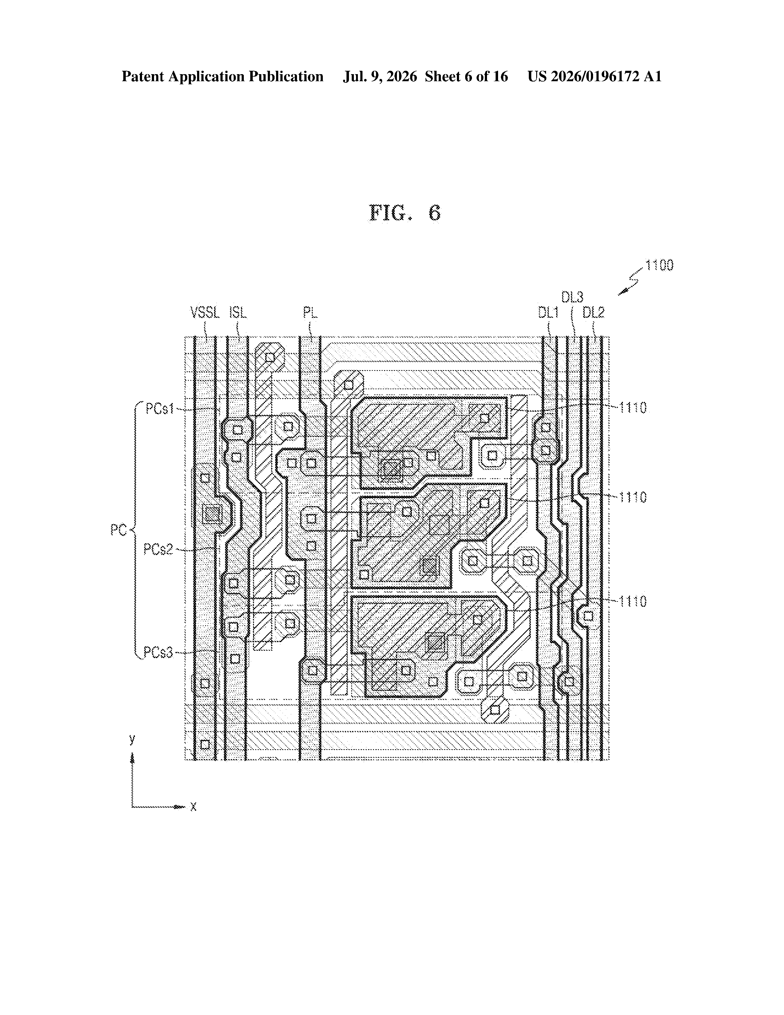
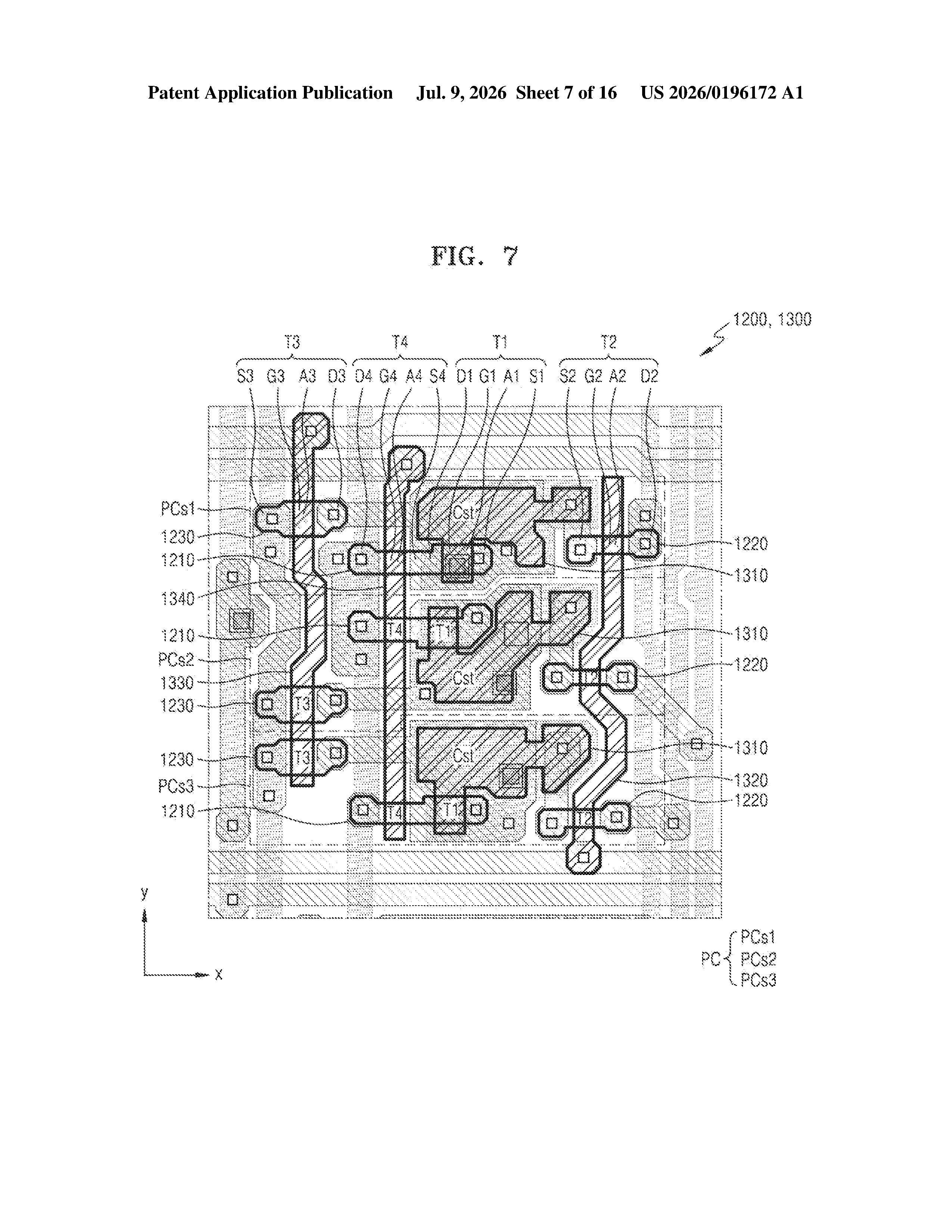
The key claim is about the first conductive pattern, which is the physical metal layer that connects the emission control transistor to the emission control line (the signal wire that tells pixels when to light up). Samsung's patent places this conductive pattern between the driving voltage line and the driving transistor in the 2D layout of the chip. That specific positioning is the novel arrangement being claimed.
The practical goal is a more compact, better-organized circuit footprint inside each sub-pixel, which matters when you're trying to fit millions of these circuits into a display panel with very little room to spare.
What this means for future Samsung OLED panels
Display panel makers compete intensely on pixel density, power efficiency, and manufacturing yield (the percentage of panels that come out of the factory without defects). A cleaner circuit layout inside each pixel can improve all three: tighter wiring reduces interference between components, a smaller footprint allows higher pixel density, and a more orderly arrangement can be easier to manufacture consistently.
Samsung Display supplies OLED panels to a wide range of device makers, including Apple for iPhones. Patents like this one represent incremental but real improvements to the underlying panel technology that eventually show up in thinner phones, longer battery life, or displays that maintain peak brightness with less power.
This is one of the least glamorous kinds of patents: a sub-pixel wiring layout with no user-visible feature and no headline product attached to it. It matters in the way that good plumbing matters. Samsung Display files patents like this routinely as part of protecting incremental manufacturing know-how, and this one doesn't signal anything particularly new in direction. Worth noting for display-industry watchers, but not for anyone else.
Get our take in your Top Stories
Liked this breakdown? Add Patentlyze as a preferred source on Google, and our plain-English take shows up more often in your Top Stories the next time Samsung patent news breaks.
There are more where this came from
We read every patent application Big Tech publishes and send you the ones worth knowing. Plain English, free, every week.
The drawings
16 drawing sheets from US 2026/0196172 A1 · click any drawing to enlarge
Want this weekly breakdown for a company we don't cover? Patentlyze Pro →