
Samsung Patents a Camera Design That Separates Pixels Unevenly to Boost Low-Light Shots
Samsung is rethinking how camera pixels are physically separated from each other inside a sensor chip, using a design where groups of four pixels share a single lens and the barriers between groups are deliberately different widths depending on where they sit.
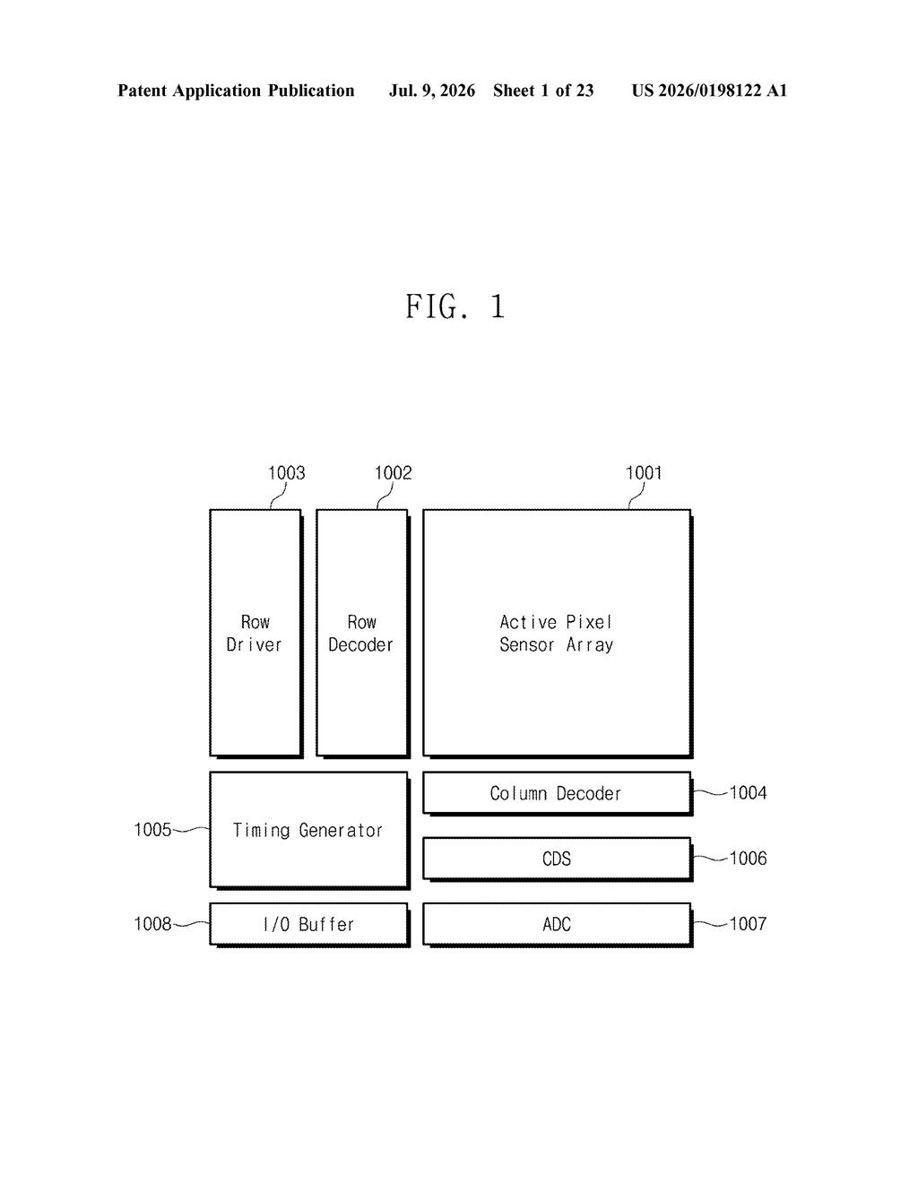
What Samsung's shared micro-lens pixel design actually does
Imagine a camera sensor as a sheet of tiny light-catching buckets, each one a pixel. Right now, most sensors treat every pixel as its own independent unit with uniform walls between each one. Samsung's patent describes a different approach: grouping four pixels together under one shared lens, like putting four apartments under one skylight.
The clever part is how the walls (called trenches) between those pixel groups are built. The outer wall that circles the whole four-pixel group is a different thickness than the inner dividers separating each pixel inside the group. Samsung engineers those width differences precisely, rather than making everything uniform.
This matters because thinner walls between pixels mean more of the sensor surface is actually collecting light instead of being blocked by physical barriers. In low-light conditions, every bit of extra light-gathering area helps your photos look cleaner and less grainy.
How the trench widths separate Samsung's pixel clusters
The patent describes an image sensor built on a silicon substrate that receives light from its back surface, a design called BSI (back-side illumination) that keeps wiring out of the light path.
Pixels are organized into 2x2 groups (four pixels arranged in a square), and each group shares a single micro lens sitting on top. Two neighboring groups are then encircled by an outer trench called the first trench, while an inner trench (the second trench) has four segments that divide the pixels within a single group from each other.
The key engineering detail: the width of the outer trench between two adjacent pixel groups is different from the width of the inner trench segments sitting between individual pixels inside a group. Both trenches contain a conductive metal pattern wrapped in an insulating layer, but they are sized independently.
- Outer trench: handles isolation between whole pixel clusters and the dark reference region at the sensor edge
- Inner trench segments: handle isolation between individual pixels inside a 2x2 group
- Variable widths: let engineers balance light collection area, electrical crosstalk (where charge leaks between pixels), and optical crosstalk (where stray light bleeds across)
The sensor also includes an optical black region, an area of pixels kept permanently dark to give the sensor a reference for true black, bordered by the same trench structures.
What this means for Samsung's next camera sensors
Camera sensors in smartphones are already physically tiny, so manufacturers are constantly looking for ways to squeeze more light-gathering efficiency out of the same chip area. By giving engineers independent control over the trench widths at different levels of the pixel hierarchy, Samsung can fine-tune the tradeoff between keeping pixels electrically separate and maximizing the area that actually catches photons. That's a meaningful lever for improving image quality, particularly in dim scenes where your phone camera tends to struggle most.
Samsung makes image sensors not just for its own Galaxy phones but for a wide range of Android devices, so improvements in sensor architecture can ripple across a large portion of the smartphone market. This particular patent looks like foundational chip-architecture work rather than a finished product feature, but that's exactly the kind of filing that shows up inside a new sensor generation a year or two later.
This is a quiet but legitimate piece of sensor engineering. Variable-width pixel isolation structures are the sort of detail that never shows up in a marketing slide but directly affects how good your nighttime photos look. It's not a flashy filing, but Samsung's sensor division produces some of the most widely used camera chips in the world, so architecture patents like this are worth tracking.
Get our take in your Top Stories
Liked this breakdown? Add Patentlyze as a preferred source on Google, and our plain-English take shows up more often in your Top Stories the next time Samsung patent news breaks.
There are more where this came from
We read every patent application Big Tech publishes and send you the ones worth knowing. Plain English, free, every week.
Want this weekly breakdown for a company we don't cover? Patentlyze Pro →