Microsoft Patents an Automated Template System for Chip Interposer Layout Design
Designing the silicon "bridge" that connects multiple chips in a modern processor package is painstaking, repetitive work. Microsoft's new patent describes a system that automates a big chunk of that layout process using reusable, snappable design templates.
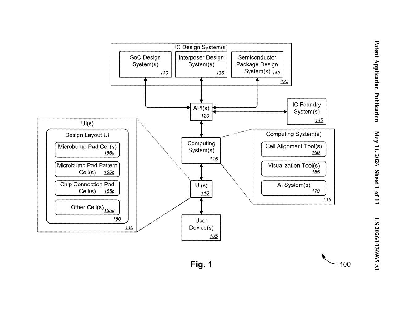
What Microsoft's interposer layout template tool actually does
Imagine you're assembling a very complex LEGO set — except instead of plastic bricks, you're connecting thousands of microscopic electrical contact points across several layers of silicon. That's roughly what chip packaging engineers do when they design an interposer: a thin silicon layer that sits between a main chip (an SoC) and the circuit board, routing signals between the two.
Right now, engineers often have to manually place and align those contact points — called microbump pads — one group at a time, making sure everything lines up perfectly across multiple layers. Microsoft's patent describes a tool that reads the existing chip design, picks the right pre-built layout template for each contact group, and automatically positions everything in the interposer design file for you.
The big idea is reusability. Once a template is built for a particular pad pattern, it can be duplicated across the same project or even reused in entirely different chip designs. That's a meaningful time-saver in an industry where design cycles are long and expensive.
How the template cell alignment system maps SoC pads to interposer layers
The system ingests a first design file from an SoC (System-on-Chip) device — essentially a map of where all the microbump contact pads are located on the underside of the chip die. These pads are organized into groups, and within each group, sets of pads share an identical spatial pattern centered on a common point.
For each of those groups, the tool automatically selects a matching template cell from a pre-built library. Each template cell contains three vertically aligned layers of information:
- A pattern of interposer microbump pads (the top side, facing the SoC chip)
- A pattern of chip connection pads (the bottom side, facing the package substrate)
- The interconnection routing through the interposer layers between those two pad sets
The critical constraint is vertical alignment — the centers of all three layers within a template cell must line up precisely. This ensures that when the SoC is physically mounted on the interposer, every contact point meets its counterpart without offset.
Once the right templates are selected, the system autonomously positions them in the interposer design file, producing output formatted specifically for manufacturing equipment. The resulting file is ready to send downstream to fabrication without manual re-entry.
What this means for advanced chip packaging design pipelines
Advanced chip packaging — the kind used in high-end processors, AI accelerators, and datacenter chips — is increasingly where the real performance gains come from. Interposers are central to designs like chiplets, where multiple smaller dies are connected on a shared silicon bridge. Automating the interposer layout step could meaningfully compress design timelines and reduce human error in a stage of the process that currently requires deep specialist expertise.
For Microsoft, which designs custom silicon for Azure infrastructure (including its Maia AI chips), tooling that speeds up the packaging design cycle has obvious internal value. The patent also signals Microsoft's growing investment in the full IC design stack — not just the chips themselves, but the software infrastructure around designing them.
This is a genuinely useful piece of EDA (Electronic Design Automation) tooling, not a flashy consumer-facing invention. The value is real but narrow: it matters most to teams doing high-volume chiplet or multi-die packaging work, where layout repetition is a known bottleneck. Given Microsoft's expanding custom silicon ambitions, building this kind of tooling in-house makes strategic sense.
Which company should we read for you?
We track 17 companies here. Pro is the same weekly breakdown for any company you choose, delivered privately. Type a name and we'll scope it and send you a quote.
Get one Big Tech patent every Sunday
Plain English, intelligent commentary, no hype. Free.
Editorial commentary on a publicly published patent application. Not legal advice.