Microsoft Patents a Way to Build FPGA Barrel-Shifters Using DSP Multipliers
FPGAs are incredibly flexible chips, but their internal resources aren't all created equal — and Microsoft has filed a patent to stop one common operation from hogging the most precious ones.
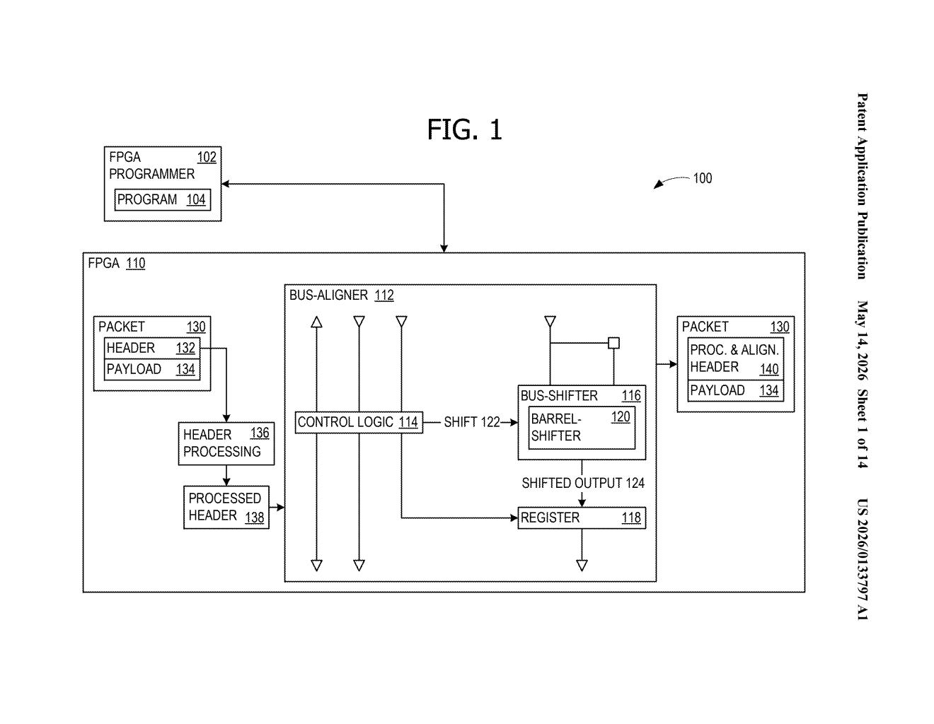
How Microsoft offloads bit-shifting from FPGA logic tables
Imagine you're packing a moving truck. You have two types of space: expensive, versatile shelving (great for almost anything) and dedicated bike racks (purpose-built, often sitting empty). Microsoft's patent is essentially a plan to strap more cargo onto those bike racks so the shelves stay free.
On an FPGA — a reprogrammable chip used in data centers and network hardware — a barrel-shifter is a circuit that slides a string of bits left or right by a set number of positions. It sounds simple, but building one traditionally eats up a lot of LUTs (lookup tables), the chip's most flexible and in-demand resource. Microsoft's approach reroutes that work to DSP multiplier blocks, which are math-focused units that often sit underused.
The result: the same bit-shifting gets done, but without crowding out other logic that really needs those LUT slots. For wide data paths — say, 256 bits at a time — this can free up a meaningful chunk of the chip's programmable fabric.
How the two-stage DSP multiplier pipeline shifts bits
The patent describes a two-stage barrel-shifter architecture built entirely out of DSP multiplier blocks, the dedicated arithmetic units baked into most modern FPGAs.
The trick is encoding the desired shift amount as a one-hot value (a binary string where exactly one bit is set to 1, making it trivially usable as a multiplier selector) and then feeding that into a DSP multiplier alongside the data. Stage one handles fine shifts — small bit offsets — using a set of parallel 8-bit DSP shifters. Stage two handles coarse shifts — larger jumps — using a second parallel set of 4-bit DSP shifters that work in tandem with the first.
For a 32-bit barrel-shifter, the design uses:
- Seven parallel 8-bit shifters in stage one
- Eight parallel 4-bit shifters in stage two
To scale up to a 256-bit shifter, the 32-bit design is applied recursively — meaning the same building block is nested inside itself. The overlapping data windows between adjacent multipliers ensure no bits get dropped at the seams between DSP blocks, which is the key engineering challenge the patent addresses.
What this means for FPGA resource budgets in data-center hardware
FPGAs are increasingly common in Microsoft's Azure infrastructure for accelerating networking, inference, and custom workloads. On those chips, LUT resources are the bottleneck — there's almost never enough of them. Any technique that shifts routine work like bit-shifting off LUTs and onto underutilized DSP blocks directly translates to more room for the logic that actually differentiates your accelerator design.
For engineers building on Azure's FPGA-backed services or designing custom FPGA IP, this kind of resource-aware architecture can be the difference between a design that fits on a given chip and one that doesn't. It's a niche optimization, but in silicon design, niche optimizations compound fast.
This is unglamorous but genuinely useful chip-design engineering. It won't make headlines outside the FPGA community, but the insight — that DSP blocks are chronically underused and can absorb work that would otherwise strain LUTs — is exactly the kind of practical optimization that shows up in shipping hardware. Worth attention if you work on FPGAs; safely ignorable if you don't.
Which company should we read for you?
We track 17 companies here. Pro is the same weekly breakdown for any company you choose, delivered privately. Type a name and we'll scope it and send you a quote.
Get one Big Tech patent every Sunday
Plain English, intelligent commentary, no hype. Free.
Editorial commentary on a publicly published patent application. Not legal advice.