Samsung Patents a Stepped Isolation Layer Design for Next-Gen 3D Memory Chips
As memory chips get more densely packed, the walls that separate individual memory cell blocks have to do more work in less space. Samsung's latest patent describes a clever stepped architecture for those dividing walls — a small structural detail that could matter a lot at the nanometer scale.
What Samsung's stepped memory boundary actually does
Imagine a city block where every building needs a firewall separating it from its neighbor. Now imagine those buildings are stacked dozens of stories high and shrinking every generation. At some point, the firewall itself becomes a structural problem.
That's roughly the challenge Samsung is tackling here. In modern 3D memory chips — like the vertical NAND and next-generation DRAM being developed today — individual memory cell blocks have to be electrically isolated from one another. The device isolation layers (think: insulating walls) that do this job need to be precisely engineered, or signals bleed between blocks and the chip fails.
Samsung's patent describes a stepped geometry for the inner isolation layer — a two-part structure with a small ledge or shelf that bridges it to an outer isolation layer. This step shape is designed to improve how well the layers fit together and insulate at the boundaries where stress and manufacturing variability are highest.
How the step portion bridges two isolation layers
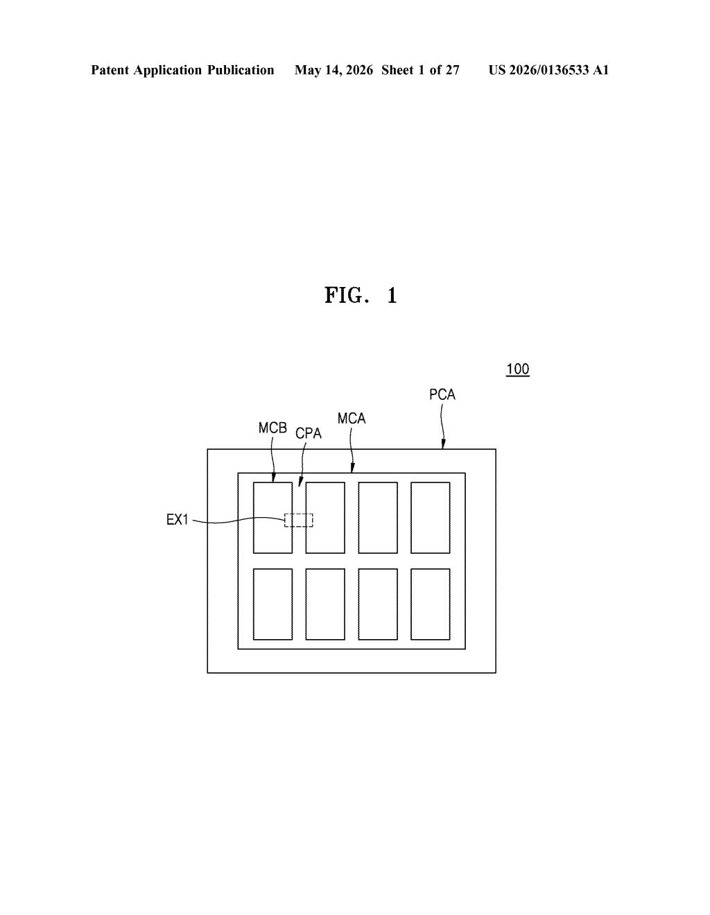
The patent covers a semiconductor memory device built around vertical channel transistors — the kind used in 3D NAND flash and emerging vertical-channel DRAM designs, where transistors are stacked vertically rather than laid flat on a silicon wafer.
Each group of transistors forms a memory cell block (MCB). Between blocks sits a boundary region whose job is to electrically isolate each block from its neighbors. Inside that boundary region, Samsung places two isolation layers side by side:
- First device isolation layer — the one closest to the active transistors. This is the novel piece: it has a first portion (a lower section), a second portion stacked on top, and a step portion — a horizontal shelf that juts out from the base of the second portion and connects to the outer isolation layer.
- Second device isolation layer — sits farther from the transistors, with the first layer in between.
The step geometry is the key claim. By creating a shelf at the junction between the two portions, Samsung changes the stress profile and the contact interface at the boundary — potentially reducing leakage current, improving structural stability during fabrication, or both. The patent doesn't specify the exact material stack but the layered geometry implies dielectric fill processes common in advanced node memory manufacturing.
What this means for DRAM and NAND density scaling
Memory density is one of the most fiercely competitive battlegrounds in semiconductors, and isolation integrity is a silent bottleneck. As cell blocks get smaller and closer together, keeping them electrically separate becomes harder — any leakage between blocks means data errors. A structural innovation in the isolation geometry, even a subtle one like a stepped profile, can be the difference between a manufacturable design and one that yields poorly.
For Samsung specifically, this kind of incremental structural patent matters for its roadmap in vertical-channel DRAM (VC-DRAM), which the company is actively developing as a replacement for conventional planar DRAM as scaling limits approach. Getting the isolation architecture right at the boundary regions is foundational to making those chips work in volume production.
This is deep-in-the-weeds process engineering — not a product feature anyone will ever see on a spec sheet. But Samsung's memory division files patents like this precisely because the structural details of isolation layers at scale are genuinely hard, and getting them wrong is expensive. It's not a flashy filing, but it's the kind of thing that determines whether next-gen VC-DRAM ships on schedule or gets delayed by yield problems.
Get one Big Tech patent every Sunday
Plain English, intelligent commentary, no hype. Free.
Editorial commentary on a publicly published patent application. Not legal advice.