Samsung Patents a Multi-Adhesive Layer Design for Stacked Semiconductor Packages
Stacking memory chips sounds simple until you realize that keeping them mechanically stable, thermally compliant, and electrically connected at microscopic scales is genuinely hard. Samsung is patenting a specific multi-layer adhesive approach to solve exactly that.
What Samsung's stacked chip adhesive system actually does
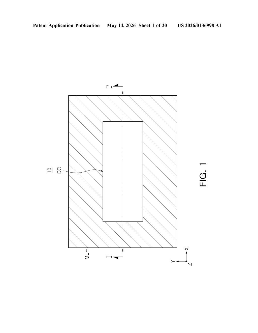
Imagine stacking several ultra-thin chips on top of each other — like a tiny club sandwich — and needing every layer to stay perfectly aligned, bonded, and electrically connected. Samsung's patent describes a semiconductor package that does exactly this, using a carefully ordered stack of memory chips wired together through tiny vertical connections called through-vias.
On top of the chip stack, Samsung adds a dummy chip — a non-functional silicon piece that exists purely for structural reasons, like a cap on the sandwich. The interesting part is how it's attached: not with a single adhesive, but with two separate adhesive layers stacked on top of each other between the chips and the dummy cap.
That two-layer adhesive approach is the core of what Samsung is protecting here. By tuning each layer independently, engineers can balance things like stress absorption and bonding strength in ways a single glue layer can't.
How the dual adhesive layers bond chips in Samsung's stack
The patent describes a 3D semiconductor package built by stacking multiple semiconductor chips vertically on a base chip. Each chip in the stack has pads on its top and bottom surfaces connected by through-vias (vertical electrical tunnels drilled through the silicon itself — essentially the wiring that lets signals pass from one chip layer to the next without going around the outside).
The stack is ordered precisely:
- A first semiconductor chip sits directly on the base chip, its lower pads touching the base chip's upper connection terminals.
- A second semiconductor chip sits on top of that, connected pad-to-pad.
- A third semiconductor chip — notably described as face-down, with its front pads contacting the second chip's upper pads — sits at the top of the active stack.
Above all of this sits a dummy chip — structurally important but electrically passive — held in place by two adhesive layers: a first adhesive layer directly on the chip stack, and a second adhesive layer on top of that.
The dual adhesive architecture is the patentable core. Each layer can be a different material with different mechanical or thermal properties, giving packaging engineers a finer-grained way to manage stress at the top of the stack — which is where warpage and delamination problems tend to originate in tall chip stacks.
What this means for high-density memory packaging
This is the kind of packaging detail that matters enormously in High Bandwidth Memory (HBM) and other stacked DRAM products, where yield and reliability live or die on how well layers stay bonded under thermal cycling. A dummy chip that shifts or delaminates can crack through-via connections below it, killing an expensive module.
For Samsung specifically, this work sits squarely in the competitive battleground of HBM production — a market where SK Hynix currently leads and Samsung has been working to close the gap. Better adhesive engineering in the cap layer is one of the unglamorous but real levers for improving yield and long-term reliability in high-stack-count packages.
This is a narrow, specific packaging patent — not a conceptual leap, but a genuine engineering detail that matters in high-volume semiconductor manufacturing. The dual adhesive layer idea is the kind of incremental-but-real improvement that separates high-yield HBM production from mediocre yield, and Samsung filing it suggests this is something their packaging teams are actively iterating on.
Get one Big Tech patent every Sunday
Plain English, intelligent commentary, no hype. Free.
Editorial commentary on a publicly published patent application. Not legal advice.