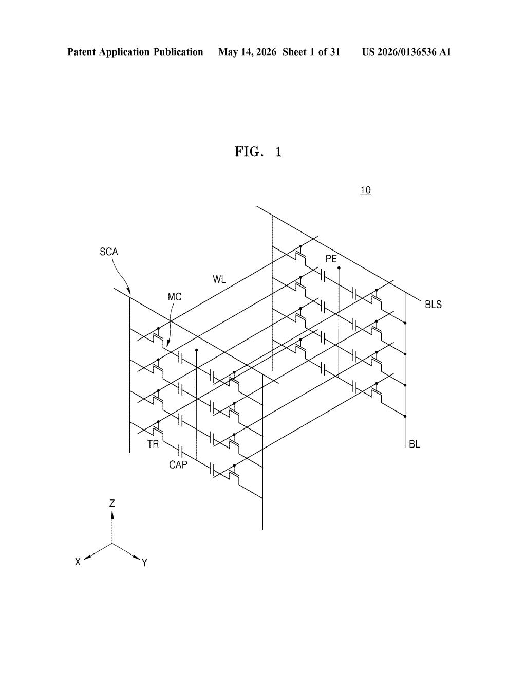
Samsung Patents a Layered Etching Process for Next-Gen Memory Chips
Samsung is patenting a precise manufacturing method for memory chips that uses alternating crystal layers as temporary scaffolding — then selectively dissolves parts of them to sculpt the final structure. It's the semiconductor equivalent of lost-wax casting, applied to nanoscale memory cells.
What Samsung's alternating-crystal memory process actually does
Imagine building a sandcastle using two different types of sand — one that washes away easily and one that doesn't. You pack them in alternating layers, carve your design, then rinse away the soft sand to reveal a perfectly shaped structure underneath. That's roughly what Samsung is doing here, but at a scale measured in nanometers.
Samsung's patented process stacks two types of semiconductor materials — a compound semiconductor (think materials like silicon-germanium) and a monocrystalline semiconductor (highly pure, single-crystal silicon) — in alternating layers. The compound layers act as temporary scaffolding. Once the structure is etched into shape, the compound material is removed, leaving only the precisely sculpted monocrystalline patterns behind.
The result is a method for creating extremely precise, three-dimensional memory cell structures. By controlling which layers get removed and how, Samsung can shape the channels and gates inside memory chips with high accuracy — which matters a lot when you're trying to pack more memory into a smaller space.
How the compound and monocrystalline layers get selectively etched
The process starts by depositing alternating layers of two semiconductor materials onto a substrate — a compound semiconductor and a monocrystalline semiconductor. Compound semiconductors are materials made from two or more elements (like silicon-germanium), while monocrystalline semiconductors are single-crystal silicon, known for its uniformity and electrical consistency.
Once the layers are stacked, they're etched in a specific direction to form two separate "molds" — essentially patterned ridges running parallel across the chip surface. The key move: the compound semiconductor patterns are then selectively removed entirely, because they etch away much faster than the monocrystalline patterns (this is called etch selectivity — the ability to remove one material while leaving another almost untouched).
Next, the monocrystalline patterns undergo isotropic etching — an etching technique that removes material equally in all directions, rounding and thinning the structures rather than just cutting straight down. An insulating layer is then deposited to fill in the gaps and surround the remaining semiconductor patterns.
- The insulating layer is etched back with high selectivity — removing it preferentially while protecting the semiconductor patterns
- Finally, at least one of the monocrystalline patterns is etched to its final form
- The result is a precisely shaped semiconductor structure suitable for a memory cell
This sequence of selective depositions and removals is how modern 3D memory structures — like those in DRAM or NAND flash — achieve their tight geometries.
What this means for future DRAM and 3D memory density
Memory chip density is one of the core battlegrounds in semiconductors right now. As traditional 2D scaling hits physical limits, chipmakers have shifted to stacking memory cells in three dimensions — and every step of that stacking process needs to be more precise than the last. Samsung's approach uses sacrificial compound semiconductor layers as geometric guides, then removes them to free up the monocrystalline structures for final shaping. That kind of controlled scaffolding is central to how you build reliable, high-density memory at advanced nodes.
For you as a consumer, this is the kind of process innovation that eventually shows up as cheaper, faster, or more energy-efficient RAM and storage in phones, laptops, and data center servers. It won't ship as a product announcement — it's a manufacturing method — but process patents like this are how Samsung defends its fab leadership against SK Hynix, Micron, and TSMC.
This is deep-fab process engineering — not the kind of patent that sparks headlines, but exactly the kind that wins memory market share. Samsung files a steady stream of these manufacturing method patents, and this one fits a recognizable pattern of work on 3D DRAM and next-generation cell structures. It's not exciting reading, but if you follow semiconductor fab competition, it's a meaningful data point about where Samsung's process R&D is focused.
Get one Big Tech patent every Sunday
Plain English, intelligent commentary, no hype. Free.
Editorial commentary on a publicly published patent application. Not legal advice.