Samsung Display Patents a Redesigned Pixel Boundary Layer for OLED Screens
The walls between pixels in an OLED screen matter more than most people realize. Samsung Display is rethinking exactly how those walls are shaped — and a continuous peripheral opening around each pixel cluster is the key move.
What Samsung's pixel-wall redesign actually changes
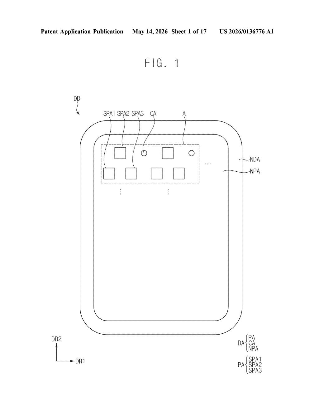
Imagine an OLED screen as a tiny city grid, where each block is a pixel and each pixel is split into three houses — one red, one green, one blue. The walls between those houses are called the pixel defining layer, and they do two jobs: keep the light-emitting materials in the right places, and prevent electrical crosstalk between neighbors.
Samsung's patent redesigns those walls so that a single, continuous peripheral opening runs along the outside boundary of each group of three sub-pixels, right where the pixel area meets the non-pixel area. Instead of each sub-pixel being completely walled off as an island, the defining layer bridges across at least two adjacent sub-pixels in one connected structure.
The practical goal is tighter control over where the organic light-emitting material lands during manufacturing, and potentially a cleaner boundary between the lit and unlit parts of the panel. It's a structural tweak, not a new material or a new type of display — but structural tweaks at this scale can meaningfully affect brightness uniformity and panel longevity.
How the peripheral opening wraps Samsung's sub-pixel edges
The patent describes a pixel defining layer (PDL) — a patterned insulating film deposited on top of the pixel electrodes in an OLED stack. The PDL's job is to expose only the intended light-emitting zone of each electrode while covering its edges, preventing current from leaking around the sides.
What's distinctive here is the introduction of a peripheral opening: a trench or gap in the PDL that is positioned in the non-pixel area (the dark border around each pixel group) and runs continuously between and around all three sub-pixel areas — red, green, and blue. Critically, the boundary of this peripheral opening is defined by tracing along the edges of all three pixel electrodes, not by cutting through independent enclosed zones.
The PDL itself is described as continuously extending across at least two adjacent sub-pixel areas, meaning it acts as a single connected structure rather than three separate walls. This is the architectural departure from more conventional PDL designs.
- Pixel area: contains the three sub-pixel electrode zones where light is emitted
- Non-pixel area: the surrounding dark region where the peripheral opening lives
- Peripheral opening: a continuous trench in the PDL that runs around the full pixel cluster boundary
- PDL coverage: the layer covers electrode edges but bridges across adjacent sub-pixels as one piece
What this means for future Samsung OLED panel quality
For display manufacturers, the shape of the pixel defining layer directly influences how organic emitter materials are deposited — whether by inkjet printing or evaporation. A continuous peripheral opening that precisely follows electrode edges can act as a capillary or containment guide, helping to keep emitter inks from bleeding into the non-pixel area and improving deposition uniformity across the panel.
For consumers, better deposition control means more consistent brightness across sub-pixels, which translates to more accurate color and potentially longer panel life before burn-in artifacts appear. This is incremental engineering, not a headline feature — but Samsung Display supplies OLED panels to Apple, Google, and its own Galaxy devices, so even small manufacturing improvements at this level propagate across hundreds of millions of screens.
This is deep-stack display engineering — the kind of filing that rarely makes headlines but quietly underpins every panel Samsung ships. The continuous peripheral opening concept is a clever structural idea for tightening deposition control, and given Samsung Display's role as a top-tier supplier, it's worth tracking even if it won't show up in a spec sheet.
Get one Big Tech patent every Sunday
Plain English, intelligent commentary, no hype. Free.
Editorial commentary on a publicly published patent application. Not legal advice.