Samsung Patents a Heat-Resistant Shielding Structure for Semiconductor Packages
Soldering chips onto circuit boards creates a heat problem — the same heat that bonds the chip can damage the shielding around it. Samsung's new patent tries to solve that with a smarter material placement.
What Samsung's chip shielding structure actually does
Imagine gluing a fragile ceramic tile onto a metal plate using hot wax — and then wrapping the tile in a protective sleeve made of the same wax. Any extra heat and your sleeve melts right along with the glue. That's roughly the kind of problem chip packaging engineers deal with.
Samsung's patent describes a semiconductor package where a shielding structure is placed along the sides of the chip — not on top, and not below — sitting at a height partway up the chip's edge. Crucially, this shielding material has a higher melting point than the solder-like connection terminals that attach the chip to its substrate (the base board it sits on).
The practical upside: when the package goes through high-heat assembly steps, the shield stays solid while the connections do their job melting and bonding. You end up with a chip that's physically protected and properly connected, without one process wrecking the other.
How the shielding layer sits beside the chip without melting
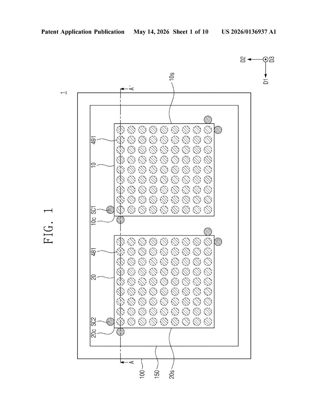
The patent claims a semiconductor package made up of three key elements: a substrate (the base), a semiconductor chip sitting on top of it, and a shielding structure positioned along the chip's side surfaces.
The geometry is specific: the top surface of the shielding structure sits at a level between the bottom and top surfaces of the chip — meaning it wraps partway up the sides, like a collar, rather than fully encasing the chip or sitting flush with the board. This partial-height placement is intentional and likely manages both electromagnetic interference (EMI) shielding and mechanical protection without interfering with the chip's top surface connections or thermal dissipation paths.
The key engineering constraint is the melting point differential: the shielding material must have a higher melting point than the connection terminals (think solder bumps or similar interconnects) between the chip and substrate. This matters because chip assembly involves reflow soldering — a process where heat is applied to melt and set those connections. If the shield melted at the same temperature, it would deform or fail during assembly.
- Substrate: the base board the chip mounts to
- Connection terminals: solder-like joints that bond chip to substrate under heat
- Shielding structure: a side-mounted collar of higher-melting-point material for protection
What this means for chip packaging reliability
Chip packaging is one of the less glamorous but increasingly critical battlegrounds in semiconductors — as chips get denser and smaller, keeping them shielded from electromagnetic noise and physically intact through assembly gets harder. Samsung is one of the world's largest chip manufacturers and packaging specialists, so patents like this reflect real production-line engineering challenges, not just theoretical ideas.
For consumers, better packaging reliability means fewer field failures in devices like phones, SSDs, and wearables — the kinds of products where Samsung's advanced packaging is already widely deployed. This specific design could simplify assembly processes or reduce defect rates in high-volume manufacturing runs.
This is a focused, incremental packaging engineering patent — the kind that quietly keeps production lines running more reliably rather than unlocking some new capability. It's not flashy, but Samsung filing this suggests they've hit a real yield or reliability issue in manufacturing and engineered their way around it. Worth a look if you follow semiconductor packaging trends; skip it if you're hunting for product announcements.
Get one Big Tech patent every Sunday
Plain English, intelligent commentary, no hype. Free.
Editorial commentary on a publicly published patent application. Not legal advice.