
Patent Targets the Invisible Errors That Corrupt Color and Detail in Digital Photos
Every digital camera sensor has a noise problem baked into its hardware. Sony's latest patent describes a circuit-level trick to reduce that noise by resetting the signal path between each pixel readout.
What Sony's image sensor noise fix actually does
When your camera captures a photo, each pixel on the sensor converts light into an electrical signal. But the electronics that read those signals can introduce their own unwanted noise, blurring fine detail or creating grain in low-light shots. This is a long-standing problem in camera hardware, and chip designers spend enormous effort trying to minimize it.
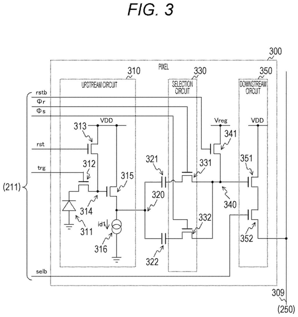
Sony's patent describes a system where two small storage units (called capacitors) take turns holding the pixel's signal. While one is being read, a tiny reset circuit clears out any leftover electrical noise from the reading path before the other capacitor connects. That brief cleaning step means the electronics start from a neutral baseline each time, which can reduce a common type of noise called reset noise.
The approach is incremental rather than radical, but these kinds of circuit-level refinements are exactly how Sony maintains its reputation for high-quality image sensors, which power cameras from iPhones to professional cinema rigs.
A downstream reset transistor initializes a level of the downstream node when both capacitive elements are disconnected from the downstream node.
Translation: A tiny electronic switch clears out residual voltage so it does not muddy the next color reading.
How the capacitor-switching circuit cleans up pixel reads
The patent covers a solid-state imaging element (the chip inside a digital camera that converts light into data) with a specific circuit arrangement for reading pixel values more cleanly.
The core architecture works like this:
- An upstream circuit samples two voltage levels from each pixel: a reset level (the baseline with no light) and a signal level (the baseline plus the effect of incoming light). Comparing these two cancels out fixed noise, a technique called correlated double sampling.
- Two capacitive elements (tiny charge-storage components) hold these two voltage levels temporarily.
- A selection circuit connects each capacitor to a shared downstream wire one at a time. Critically, both capacitors are briefly disconnected between connections, and during that gap a downstream reset transistor clears the wire to a known voltage.
- A downstream circuit then reads each voltage level off the wire in sequence and passes the data along.
The key insight is that resetting the downstream wire between the two reads prevents charge left over from the first read from contaminating the second. This reduces reset noise, a form of random electrical variation that is otherwise hard to eliminate in analog readout chains.
What this means for Sony's camera sensor business
Sony Semiconductor Solutions supplies image sensors to a large portion of the smartphone industry, including Apple, as well as to camera makers and automotive companies. Improvements at the circuit level, even modest ones, compound across billions of pixels read every second in a modern sensor, making real differences in low-light performance and dynamic range for everyday users.
This patent sits in the middle of very competitive territory. Samsung, OmniVision, and others are all chasing the same noise-reduction goals. For Sony, filing patents on specific readout architectures helps protect the circuit designs that differentiate its sensors, and may show up in future generations of its popular Exmor sensor family.
This is unglamorous but real engineering work. Noise reduction at the readout circuit level is one of the main battlegrounds in image sensor design, and Sony has the most to gain from protecting incremental wins here. It won't generate consumer headlines, but it's exactly the kind of patent that shapes which camera sensors end up in your next phone.
There are more where this came from
We read every patent application Big Tech publishes and send you the ones worth knowing. Plain English, free, every week.
The drawings
40 drawing sheets from US 2026/0230729 A1 · click any drawing to enlarge


Want this weekly breakdown for a company we don't cover? Patentlyze Pro →
Be the first to weigh in