Samsung Patents an On-Chip Circuit for Testing Interconnect Health
As chips get smaller and the wires connecting their components shrink to nanometer scales, verifying those connections without destroying the chip becomes a serious engineering puzzle. Samsung's latest patent embeds the testing equipment directly into the chip itself.
What Samsung's built-in interconnect tester actually does
Imagine buying a new appliance, only to find out it occasionally fails because of a tiny, invisible wire inside that's slightly too resistive or has a small electrical leak. Detecting that kind of flaw normally requires specialized external equipment — and by the time you find it, the device may already be in your hands.
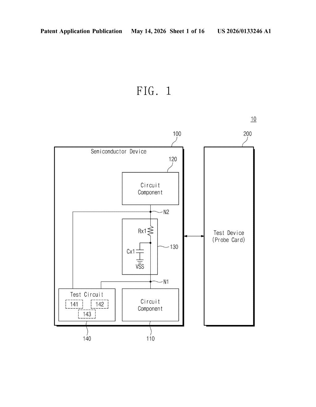
Samsung is patenting a smarter approach: a test circuit built directly onto the semiconductor chip that can measure the health of the wires (called interconnects) running between components on that same chip. Think of it like embedding a multimeter inside the chip so it can check its own wiring.
The circuit specifically measures two key electrical properties — resistance (how much the wire fights the flow of electricity) and capacitance (how much the wire unintentionally stores charge). Both can signal defects or degradation, and catching them early means fewer bad chips reaching customers.
How the test circuit measures RC values on the interconnect
The patent describes a semiconductor device that pairs two circuit components — essentially functional blocks on a chip — connected by an interconnect (the metal wire or trace linking them). Sandwiched between those components and the interconnect is a dedicated test circuit.
The test circuit's job is to measure two fundamental electrical properties of the interconnect:
- Resistance component — how much the wire impedes current flow, which can indicate thinning, corrosion, or poor material deposition
- Capacitance component — how much parasitic charge the wire accumulates, which can slow signal propagation or cause cross-talk between adjacent wires
By positioning the test circuit directly between both circuit components and the interconnect, Samsung ensures measurements reflect the actual in-circuit behavior of the wire — not an approximation taken from a separate test structure elsewhere on the wafer.
The design is meant to interface with an external test device (such as a probe card — a tool with tiny pins that contact the chip during manufacturing) to read out those measurements, enabling automated quality screening during production.
What this means for chip yield and manufacturing quality
For chip manufacturers, interconnect defects are one of the leading causes of yield loss — the percentage of chips that pass quality control. As process nodes shrink below 5nm and 3nm, interconnect wires become so thin that tiny variations in deposition or etching can push resistance or capacitance out of spec. Catching those failures early, before chips are packaged and shipped, saves significant cost.
For Samsung specifically, this kind of in-situ (on-chip) testing capability could strengthen its foundry competitiveness by improving yield predictability. If the test circuit can be queried during wafer-level testing or even in the field, it also opens the door to post-deployment reliability monitoring — knowing when a chip's internal wiring is starting to degrade before it causes a system failure.
This is solid, unglamorous semiconductor engineering — exactly the kind of incremental yield-improvement work that separates competitive chip fabs from struggling ones. It's not a flashy AI or memory patent, but tighter interconnect quality control at scale translates directly into better margins and fewer field failures. Worth a quiet nod of respect.
Get one Big Tech patent every Sunday
Plain English, intelligent commentary, no hype. Free.
Editorial commentary on a publicly published patent application. Not legal advice.