Samsung Display Patents a Semiconductor Layer Layout to Reduce Signal Interference
Samsung Display is patenting a specific physical arrangement of semiconductor regions inside a display panel — one where a key semiconductor portion is deliberately kept from sitting directly above the data line beneath it. It sounds like a small structural detail, but in display engineering, stack geometry like this can be the difference between a pixel that performs cleanly and one that doesn't.
What Samsung's non-overlapping semiconductor layout actually does
Imagine a multi-story building where the electrical wiring on the ground floor runs directly under the offices above — and that proximity causes interference. That's roughly the problem Samsung is solving here.
Inside a display panel, there are stacked layers: conductive lines at the bottom carrying data, drive voltage, and initialization signals, and semiconductor regions above them that control how each pixel turns on. This patent describes a specific arrangement where the semiconductor region connected to the data line is not positioned directly above the data line itself. By avoiding that vertical overlap, Samsung can reduce the chance of parasitic capacitance or unwanted coupling between the two layers.
Parasitic capacitance is essentially an unintended electrical interaction between two conductors sitting close together — it can slow signals down or distort them. In a high-resolution display firing millions of pixels at high refresh rates, keeping these interactions under control matters for image accuracy and consistency.
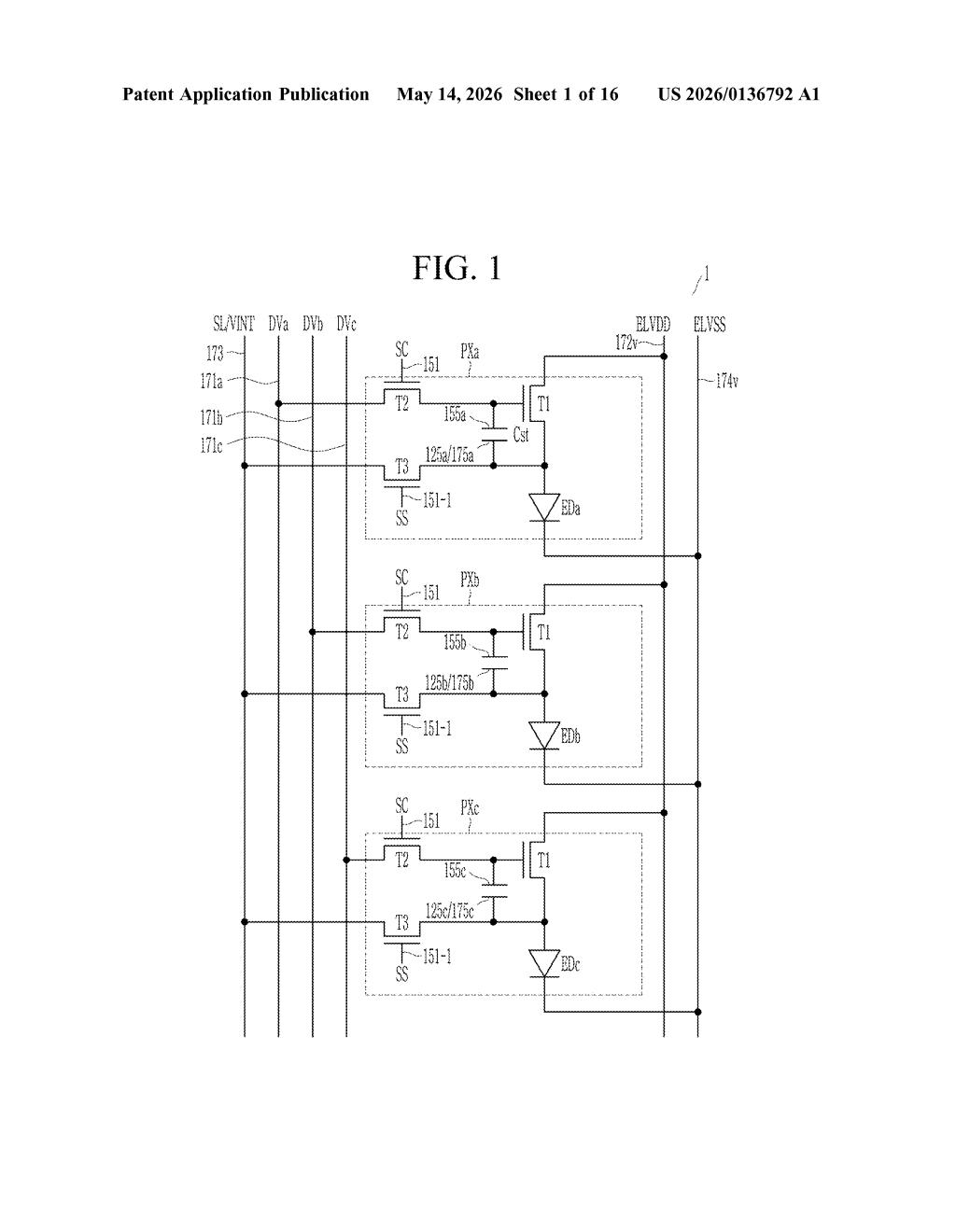
How Samsung's three-portion semiconductor layer is wired
The patent describes a display device built on a substrate with two key layers stacked on top of each other:
- First conductive layer: Contains the data line (carries pixel programming signals), the initialization voltage line (resets pixel state before each frame), and the driving voltage line (provides the current that lights up the pixel).
- Semiconductor layer: Sits on top of the conductive layer and is divided into three separate portions — each electrically connected to one of those three conductive lines respectively.
The critical claim is that the second semiconductor portion — the one tied to the data line — does not overlap the data line when viewed straight down through the stack (i.e., in the direction perpendicular to the substrate surface).
This non-overlapping geometry is the heart of the invention. In thin-film transistor (TFT) display stacks, when a semiconductor region sits directly above a conductive line, the two can form an unintended capacitor. By laterally offsetting the second semiconductor portion from its corresponding data line, Samsung aims to minimize that coupling effect.
The arrangement applies to what appears to be a pixel circuit likely used in OLED displays, where precise control of initialization and drive currents is critical for uniform brightness and accurate color.
What this means for next-gen OLED display quality
For consumers, this kind of structural refinement is invisible — but it feeds directly into display metrics you do notice, like uniformity, motion clarity, and gray-scale accuracy at high refresh rates. Samsung Display supplies panels to a wide range of device makers, so improvements at this foundational layer can ripple across smartphones, tablets, and monitors.
From a competitive standpoint, display panel engineering has become an arms race fought at the micron level. Patents like this one represent the incremental, cumulative work that separates premium panels from commodity ones. It's not a single dramatic leap — it's the kind of careful stack optimization that compounds over generations of display design.
This is a narrow, structural manufacturing patent — the kind that rarely makes headlines but quietly underpins Samsung Display's panel quality advantage. It's not a new display technology or a novel material; it's a geometric optimization in a pixel circuit stack. Worth noting if you follow display engineering closely, but not something that signals a product shift on its own.
Get one Big Tech patent every Sunday
Plain English, intelligent commentary, no hype. Free.
Editorial commentary on a publicly published patent application. Not legal advice.