
Meta Patent Reveals Invisible Circuits Embedded Directly Into Clear Eyeglass Lenses
Putting electronics inside eyeglass lenses without making them look like a screen is one of the harder unsolved problems in wearables. Meta thinks the answer is in how you shape the invisible circuits etched into the glass.
What Meta's invisible lens circuitry actually does
Ever wondered why smart glasses always look a little off, like there's something going on inside the lens? A big part of the problem is that adding any kind of electronic layer to a lens means adding conductive material, and that material tends to form visible patterns, grids, or lines that catch the light.
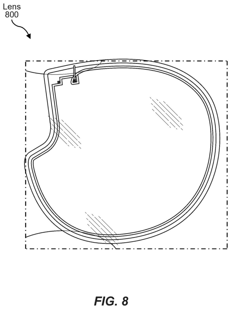
Meta's patent describes a way to coat a clear lens with a transparent conductive material and then carve it into electrode shapes that deliberately avoid clean geometric outlines. No neat squares, no repeating grids. The idea is that irregular, organic-looking shapes are much harder for the human eye to pick up on, especially in a lens you're actually wearing.
The electrodes could be used to drive features like adjustable focus, eye-tracking sensors, or other lens-level electronics. The key is that from the outside (and from your perspective looking through the lens), the circuitry stays invisible.
the transparent conductive coating is patterned into at least one conductive island that: is configured as an electrode; comprises a non-geometrically defined shape; and is separated from adjacent conductive material by an insulating gap.
Translation: The lens contains invisible, irregularly shaped electrical circuits that are isolated from each other to function.
How the non-geometric electrode pattern stays hidden
The patent describes an ophthalmic lens assembly (a technical term for a corrective or protective eyeglass lens) that has two main layers: a clear substrate (the lens itself) and a transparent conductive coating on top of it.
That coating is then patterned, meaning sections of it are etched or removed, to create isolated conductive islands. Each island acts as an electrode, which is just a point where electricity can be applied or sensed. The gap between one island and the next is an insulating gap, meaning no current flows between them accidentally.
The key technical claim is the shape of those islands. Instead of regular geometric forms like squares or hexagons (which form visible, repeating grids), the patent specifies non-geometrically defined shapes. These are irregular outlines with no clean repeating pattern. Irregular boundaries are much harder for the human visual system to detect, especially against the uniform background of a clear lens.
Practically, this means:
- The conductive layer can span most of the lens area without obvious visual artifacts
- Multiple isolated electrodes can coexist on a single lens without shorting together
- The same lens can potentially carry signals for eye-tracking, focus adjustment, or other electronic functions
An ophthalmic lens assembly includes a transparent ophthalmic substrate with a transparent conductive coating on the substrate. The transparent conductive coating is patterned into at least one conductive island that is configured as an electrode …
Translation: This device uses a clear lens coated with a special material that acts as an electrical sensor or contact point.
What this means for the future of smart glasses
For smart glasses to go mainstream, they have to look like glasses first. Any visible electronics layer, even a faint grid, immediately signals to everyone around you that you're wearing a screen. Meta is working on this optical invisibility problem at the substrate level, which is the most direct path to lenses that can do things without looking like they do.
This kind of lens-level circuitry shows up across interesting tech patents in the AR and wearables space, and Meta's specific approach here, using irregular electrode geometry rather than just thinner grids, is a materials science angle that has to be solved before a lot of other features can ship in a consumer product.
The ship path on this one is long. Transparent conductive coatings already exist (ITO glass is everywhere), but patterning them at the precision described here, across a curved optical surface, without introducing distortion or haze, requires manufacturing processes that are not off-the-shelf. Meta would need to demonstrate yield at scale, prove the electrodes survive lens finishing steps like edging and coating, and integrate them with whatever driving electronics sit in the frame. This is foundational materials work, probably several steps removed from a product announcement, but it is the right problem to solve if consumer AR glasses are the goal.
There are more where this came from
We read every patent application Big Tech publishes and send you the ones worth knowing. Plain English, free, every week.
The drawings
18 drawing sheets from US 2026/0236098 A1 · click any drawing to enlarge


Want this weekly breakdown for a company we don't cover? Patentlyze Pro →
Be the first to weigh in