
Samsung Patents Chip That Automatically Translates Memory Requests Into the Right Commands
Samsung has filed a patent for a memory architecture where the controller, not the main processor, figures out exactly how to talk to memory, potentially saving the CPU from doing that translation work itself.
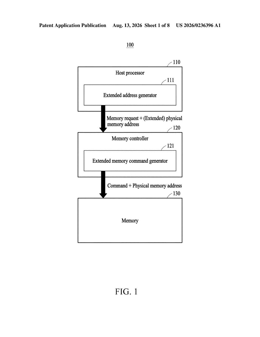
How Samsung's memory address trick offloads the CPU
Your phone or laptop's main chip currently has to handle a lot of bookkeeping when it reads or writes data to memory. It needs to know not just where data lives, but how to ask for it depending on what kind of memory is being used. That overhead adds up.
Samsung's patent describes a system where a separate memory controller takes on that job. The processor hands over a memory address, and the controller figures out which memory mode applies and translates that into the right command for the actual memory chip. The processor doesn't need to know the details of each memory type, it just makes a request and moves on.
For everyday users, this kind of design could mean a device that handles multiple memory types without the main chip getting bogged down in translation work. It's the sort of behind-the-scenes efficiency that shows up as faster, more responsive hardware, especially in devices that mix different memory technologies on the same board.
… a memory controller, separate from the host processor, configured to generate the physical memory address and a memory device command according to the target memory mode mapped to the memory address based on the memory request and the memory address received from the host processor …
Translation: A dedicated controller sits between the main processor and memory to translate requests into specific hardware commands.
How the controller maps addresses to modes and commands
The patent describes a three-part system: a host processor, a memory controller, and a memory device.
The host processor generates a memory address, essentially a label saying 'I need to read or write data here.' But that address is special: it's part of an extended memory address space, meaning different address ranges are mapped to different memory modes (think of modes as different dialects that different types of memory chips speak).
The memory controller sits in the middle and does the heavy translation work. When it receives an address and a request from the processor, it looks up which memory mode that address belongs to, then generates both the correct physical memory address (the actual hardware location) and the specific command the memory chip needs to receive. Different memory technologies, such as standard DRAM versus newer or specialized memory types, may require different command formats entirely.
The memory device at the far end simply receives the translated command and physical address and executes them. The key architectural claim is that the host processor's operating system kernel doesn't need to understand the specifics of each memory type, that complexity is abstracted away into the controller layer.
Disclosed are a device and method with memory request processing using an extension of a memory address space. An electronic device includes a host processor configured to generate a memory request and a memory address that is mapped to a target memory mode that is any one of available memory modes …
Translation: The system uses a special memory address map to tell the hardware exactly which mode to use for each data request.
What this means for chips handling mixed memory types
Chips are being asked to work with a growing variety of memory technologies at once, from traditional DRAM to high-bandwidth memory to newer non-volatile options. Managing all of those different protocols at the processor level adds software complexity and can slow things down. Offloading that translation to a dedicated memory controller keeps the main processor focused on actual computation.
For Samsung, which manufactures both the processors and the memory chips that go into phones, tablets, and data center servers, having a clean architectural patent in this area matters. The latest Big Tech patents in semiconductor memory architecture show a clear push toward separating memory management from core compute, and this filing fits squarely into that trend.
The reader-level payoff here is indirect but real: if a device's main chip spends less time managing memory bookkeeping, more of its processing budget goes toward the tasks you actually care about. The patent doesn't promise a specific product improvement, but it describes the right kind of abstraction layer for a world where single devices increasingly combine multiple memory types on the same die or package. Samsung filing this at the controller-architecture level, rather than as a software driver tweak, suggests the company wants the efficiency gain baked into silicon.
There are more where this came from
We read every patent application Big Tech publishes and send you the ones worth knowing. Plain English, free, every week.
The drawings
8 drawing sheets from US 2026/0236396 A1 · click any drawing to enlarge


Want this weekly breakdown for a company we don't cover? Patentlyze Pro →
Be the first to weigh in