
Samsung Patents a Camera Chip That Stores Light Data Differently Across Each Shot
Samsung has filed a patent for an image sensor that uses two structurally different capacitors side by side, letting each pixel store electric charge in a configuration tuned independently of its neighbor.
What Samsung's multi-layer capacitor sensor actually does
Imagine your phone camera trying to capture a scene where one part of the frame is blazing sunlight and another is deep shadow. The sensor has to hold a huge range of charge levels without overflowing or losing detail, and the tiny storage cells inside each pixel are often the bottleneck.
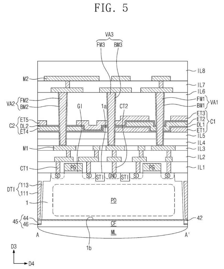
Samsung's patent describes an image sensor where two different capacitors sit next to each other on the chip, each built with a different number of electrode layers. Think of them like layered sandwiches where one has more fillings than the other. Because they have different layer counts, they can hold different amounts of charge, giving the sensor more flexibility in how it handles bright and dark areas at the same time.
This is a design tweak at the hardware level inside the sensor chip itself, not a software filter or post-processing trick. The goal is to give each pixel more headroom to capture what's actually in the scene rather than clipping highlights or crushing shadows.
… wherein the first capacitor comprises N electrodes and M dielectric layers including a first dielectric layer, wherein the second capacitor comprises L electrodes and T dielectric layers including a second dielectric layer …
Translation: The two storage components use different numbers of internal layers to hold light data.
How the electrode stacking arrangement works per pixel
The patent describes an image sensor built on a substrate that contains pixels, each with a photodiode (the light-collecting element). Above those photodiodes, the chip includes two separate capacitors spaced apart horizontally.
The key structural difference is that the first capacitor uses N electrodes (three or more, stacked vertically) separated by dielectric layers, while the second capacitor uses L electrodes (a different count, as few as two). Because the number of electrodes differs, the two capacitors have different charge-storage geometries sitting over different pixels.
This matters because capacitance in image sensors determines full-well capacity, the maximum charge a pixel can hold before it saturates and loses information. By varying the capacitor architecture pixel to pixel, the design can support:
- Different sensitivity levels across neighboring pixels
- More storage headroom in pixels expected to receive bright light
- A compact footprint, since the stacking is vertical and the capacitors are connected to the circuit below via individual vias (tiny vertical wire connections)
The claim also specifies that at least part of each capacitor overlaps its corresponding photodiode in the vertical direction, keeping the overall sensor area tight.
… a first capacitor and a second capacitor spaced apart from each other on the substrate; a first via connected to the first capacitor; and a second via connected to the second capacitor …
Translation: The sensor uses separate pathways to connect each storage capacitor to the substrate.
What this means for high-dynamic-range camera sensors
For engineers designing camera sensors used in smartphones, automotive cameras, or security systems, fitting more charge storage into a shrinking pixel footprint is one of the harder physics problems in the field. This patent's approach of varying the electrode count between adjacent capacitors is a structural answer to that problem, keeping the chip area compact while potentially widening the dynamic range each sensor can handle.
For consumers, the downstream effect would show up in photos and video that hold detail in both the bright sky and the dark foreground at the same time, without software doing the heavy lifting. Samsung's camera chips power a wide range of devices beyond its own Galaxy phones, so design choices baked into the sensor architecture can ripple across the industry. Coverage of new Big Tech patents in image sensor engineering has been picking up as manufacturers push pixel sizes smaller while demanding wider dynamic range.
Samsung's 93rd filing we've tracked in our camera sensor push since May builds on ideas like the reframing lock and the color-sorting chip lens.
The tradeoff is real. Building two slightly different capacitors side by side on the same tiny chip is fiddly work, and if even a small percentage of chips come out faulty, the cost of making each good one shoots up fast.
But the tradeoff looks worth it. Processing bright-and-dark photos in software drains your battery and can smear the image in subtle ways. A camera sensor that handles the problem on its own hardware, without getting physically bigger, is a cleaner fix than piling more software tricks onto a sensor that was already struggling.
There are more where this came from
We read every patent application Big Tech publishes and send you the ones worth knowing. Plain English, free, every week.
The drawings
21 drawing sheets from US 2026/0247736 A1 · click any drawing to enlarge


Want this weekly breakdown for a company we don't cover? Patentlyze Pro →
Be the first to weigh in