
Samsung Patents a Chip-Level Lens That Sorts Light by Color and Direction Simultaneously
Samsung has filed a patent for an image sensor that replaces traditional physical optics with a surface of microscopic nano-structures, capable of sorting incoming light by both color and polarization direction at the same time, all within a layer thinner than a human hair.
What Samsung's nano-lens camera chip actually does
A photographer points a lens at a sunlit window and gets a washed-out, glare-filled image. What the camera failed to do is distinguish between the pure colors of the scene and the polarized reflections bouncing off the glass. That difference matters, and current sensors can't sort it out on their own.
Samsung's patent describes an image sensor with a layer of nano-scale structures etched above the light-catching pixels. Instead of relying on colored plastic filters stacked on top of pixels, these tiny structures physically bend and redirect light, routing red, green, and blue wavelengths to the right pixels. At the same time, some of those structures split light by its polarization (the direction it vibrates), sending horizontally polarized light one way and vertically polarized light another. That means a single sensor can capture color and polarization data in one shot, without extra hardware.
For you as a user, this could mean cameras that see through glare automatically, detect surface textures more accurately, or produce images with richer depth information, all from a thinner, simpler sensor stack.
… a nano-photonic lens array including a plurality of unit meta-groups, each of the plurality of unit meta-groups including a first meta-region corresponding to the first pixel, a second meta-region corresponding to the second pixel, a third meta-region corresponding to the third pixel, and a fourth meta-region corresponding to the fourth pixel …
Translation: The system uses tiny patterned regions directly above groups of four pixels to bend and sort incoming light.
How the nano-structures split wavelengths and polarization
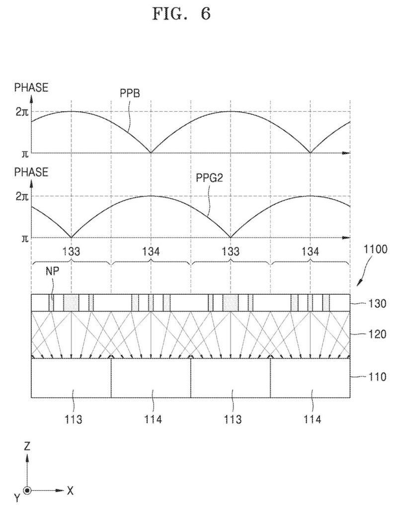
The patent describes a nano-photonic lens array: a flat layer of nano-scale pillars or ridges, each precisely shaped and spaced to manipulate how light bends around them. This is a form of meta-optics (engineered surfaces that control light using structures far smaller than the wavelength of the light itself), and it replaces the conventional color filter array that sits on top of most image sensors today.
The sensor substrate is divided into groups of four pixels. Each group handles three colors: a first wavelength (likely near-infrared or red), a second wavelength (likely green), and a third wavelength (likely blue). The nano-structures above each pixel group are tuned to focus the right color onto the right pixel.
The clever addition is polarization separation. Within each four-pixel group, two of the nano-regions contain polarization-separating nano-structures. These structures split the first-wavelength light into two components based on the angle at which it vibrates:
- Light vibrating in one direction (first polarization) goes to the first pixel.
- Light vibrating at 90 degrees to that (second polarization) goes to the fourth pixel.
Capturing both polarization states simultaneously lets the sensor compute how much of a scene's light is reflected glare versus genuine scene color, a calculation normally requiring moving parts or multiple exposures.
… at least one nano-structure provided in at least one of the second meta-region and the third meta-region is a polarization-separating nano-structure configured to provide the light of the first wavelength having a first polarization component to the first pixel and provide the light of the first wavelength having a second polarization component to the fourth pixel …
Translation: Certain microscopic pillars split the light waves so that different polarization angles reach separate pixels.
What this means for mobile and computational cameras
For mobile camera engineers, combining color filtering and polarization detection into a single, flat nano-structured layer removes the need for separate polarizing filters or multiple sensor passes. That simplification could mean thinner camera modules and faster capture, which are the two things phone makers argue about most when designing slim devices.
The broader implication sits in computational photography and machine vision. Polarization data helps algorithms separate surface reflections from subsurface detail, which matters for medical imaging, autonomous vehicle cameras, and AR headsets that need to understand real-world surfaces. Samsung's image sensor patent sits alongside a wave of sensor-level optical engineering filings tracked across the latest Big Tech patents, where companies are betting that shrinking optical work onto the chip itself is the next frontier for camera hardware.
Samsung's 91st filing we've tracked since May builds on one removing voice from recordings and one keeping 3D motion sharp in our growing look at Samsung's camera sensor work.
The tiny structures that sort light here must be built almost perfectly. A pillar even slightly too short or too wide sends light to the wrong spot on the sensor, so making millions of these chips without defects is a serious problem. Samsung is betting that its factories can hit that precision at the scale of a smartphone camera.
That bet makes sense for high-end phones, where richer, more detailed photos justify the extra cost and effort. For cheaper, mid-range phones, a simpler, older design does the job fine and costs far less.
There are more where this came from
We read every patent application Big Tech publishes and send you the ones worth knowing. Plain English, free, every week.
The drawings
41 drawing sheets from US 2026/0247732 A1 · click any drawing to enlarge


Want this weekly breakdown for a company we don't cover? Patentlyze Pro →
Be the first to weigh in