
Samsung Patents a Camera Chip That Captures Sharper Photos With Less Noise
Samsung has filed a patent for an image sensor pixel that uses five separate control transistors instead of the three that most camera sensors rely on today. The extra headroom could allow each pixel to do more without the usual compromises.
What Samsung's five-transistor pixel design actually does
You're shooting a photo in a dim restaurant and the picture comes out grainy, blotchy, or weirdly colored. That noise usually traces back to how each tiny pixel in the camera sensor reads and reports the light it captured. The more precisely a pixel can be controlled, the cleaner the image.
Samsung's patent describes a pixel design where five separate little switches, called transistors, manage how each pixel handles the electrical signal after light hits it. Standard pixels use three of these switches. Having five means the sensor can separate out different jobs, like resetting the pixel, reading its value, and selecting which row gets read, with more flexibility and less interference between those tasks.
The practical upside is that sensors built this way could read image data more cleanly, especially in tricky lighting. It's a structural change inside the sensor chip itself, not a software trick.
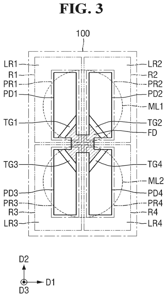
… a first photoelectric conversion element (PD) disposed on the first region; a first microlens covering the first PD; a floating diffusion region (FD) electrically coupled to the first PD; a first transfer transistor electrically coupled between the first PD and the FD …
Translation: The sensor uses a tiny lens and specialized electronic components to convert incoming light into a digital signal.
How the extra transistors divide up pixel control duties
The patent describes an image sensor built around a pixel architecture that places five transistors alongside each photoelectric conversion element (the light-detecting component, called a PD). A photoelectric conversion element works by turning incoming photons into an electrical charge.
Here's how the components connect:
- The photoelectric conversion element (PD) absorbs light and builds up a charge.
- A transfer transistor moves that charge into a small holding area called the floating diffusion region (FD).
- Five additional pixel transistors are all wired to that floating diffusion region, and at least three of them fill the three standard roles: resetting the pixel (clearing old charge), selecting the pixel (choosing which one to read), and driving the output signal (amplifying it for readout).
The key detail is that none of those five pixel transistors is a transfer transistor. Transfer is handled separately. That means the five transistors are free to be assigned to other control and readout duties, giving circuit designers more options for how to manage noise, timing, and signal strength within a single pixel.
Microlenses sit on top of each PD to focus incoming light onto the sensitive area, a standard part of modern sensor design. The patent specifies this layout at the substrate level, meaning it describes the physical silicon structure, not just a software or firmware approach.
… first to fifth pixel transistors, each electrically coupled to the FD, the first to third pixel transistors each being selected from the group consisting of a reset transistor, a selection transistor, and a driving transistor, and none of the first to fifth pixel transistors being a transfer transistor.
Translation: The design uses five specific transistors to manage the electrical charge for each pixel without using a transfer transistor.
What this means for Samsung camera sensors in phones
More transistors per pixel is a real engineering lever for image quality. Extra transistors let sensor designers separate electrical tasks that would otherwise share a wire and interfere with each other, which is one of the main sources of read noise (the random static that makes low-light photos grainy). For Samsung, which supplies image sensors to both its own Galaxy phones and many other device makers, improvements at this foundational level can ripple across a wide product range.
The tradeoff is real: more transistors per pixel means each pixel takes up more physical space on the chip, or the pixel has to shrink to keep the sensor the same size. Shrinking pixels typically means each one captures less light, which can hurt the very image quality you were trying to improve. That tension is the central engineering gamble in this design. Samsung's camera sensors already appear across a broad slice of the mobile market, so filings like this one show up regularly in the plain-English patent summaries tracking semiconductor and imaging chip development.
This is the 103rd Samsung filing we've tracked since May in our camera sensor work watchlist, building on bright and dark scene cameras and AI sharpening blurry photos.
Adding a fifth circuit switch to a pixel forces the light-collecting surface to shrink, because every new component competes for the same tiny patch of silicon. A smaller window for light means worse photos in dim rooms, which is precisely the weakness this design sets out to fix. The bet is that cleaner electrical signals from better-organized circuitry can recover more shadow detail than the reduced collector loses.
That logic holds in principle, but the math has to work at a scale smaller than a human hair, and this filing describes the architecture without proving the numbers land in the camera's favor. The ambition is coherent and the direction makes sense, but the trade only reads as worth it if Samsung can compress the geometry without letting the light penalty swallow the gains.
That is a manufacturing problem, not a drawing-board one, and no patent solves it on paper.
Get our take in your Top Stories
Liked this breakdown? Add Patentlyze as a preferred source on Google, and our plain-English take shows up more often in your Top Stories the next time Samsung patent news breaks.
There are more where this came from
We read every patent application Big Tech publishes and send you the ones worth knowing. Plain English, free, every week.
The drawings
38 drawing sheets from US 2026/0255704 A1 · click any drawing to enlarge


Want this weekly breakdown for a company we don't cover? Patentlyze Pro →
Be the first to weigh in