
Sony Patents a Microscopic Surface That Converts Display Colors More Efficiently
Sony has filed a patent for a microscopic surface layer that could make color conversion in displays far more efficient by using tiny engineered structures tuned to absorb and re-emit exactly the right light frequencies.
What Sony's color-converting nano layer actually does
Every time your TV or phone screen shows you a deep, saturated red or a vivid green, something has to convert raw light into those specific colors. That conversion process has always wasted some energy and can limit how sharp and bright a display gets.
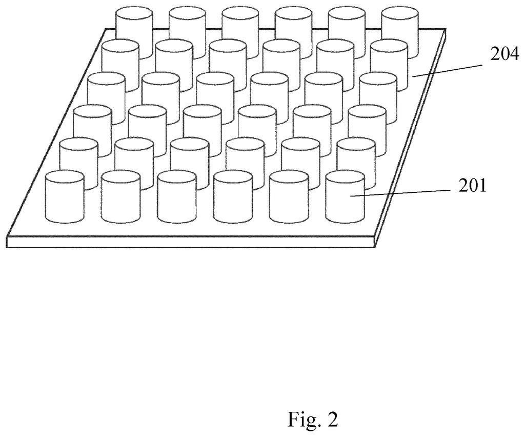
Sony's patent describes a special surface, called a metasurface, that is covered in nano-scale structures. These structures are so precisely shaped and sized that they resonate at exactly the same frequency as the light the color-converting material next to them absorbs and emits. Think of it like tuning two guitar strings to the same note so one naturally amplifies the other.
The result is a more efficient handoff between the light source and the color-converting layer. Less energy is lost in the process, which could translate to displays that are brighter, more color-accurate, or draw less power to do the same job.
… configured to absorb and emit light in the visible range, and wherein the metaatoms are configured so that they resonantly match with the frequency of the light absorbed and emitted by the emissive system …
Translation: The tiny particles are tuned to match the exact frequencies of visible light.
How metaatoms and emitters lock onto the same light frequency
The patent describes a structure called an emissive metasurface, combining two key parts:
- Nanostructured dielectric component: A non-metallic layer packed with tiny engineered shapes called metaatoms. These are not actual atoms in the chemical sense but nanoscale physical structures, each precisely designed to interact with specific wavelengths of light.
- Emissive system: A layer of material that absorbs light at one frequency and re-emits it at another, which is the core mechanism of color conversion in many display technologies.
The critical feature is resonant matching: the metaatoms are shaped so their natural optical resonance (the frequency at which they most strongly respond to light) aligns with the absorption and emission frequencies of the emissive material sitting alongside them. When frequencies match, the structures effectively couple, meaning energy transfers between them more completely rather than scattering away as heat or stray light.
In practical terms, the emissive system does not have to work as hard because the metaatoms create a local environment that encourages faster, more efficient light emission. This is related to a well-known physics principle called the Purcell effect, where a resonant structure near an emitter can accelerate how quickly the emitter releases photons.
What this could mean for next-generation display panels
Display makers have been chasing more efficient color conversion for years, particularly as microLED and quantum-dot displays push for higher brightness and lower power draw. A surface layer that passively improves conversion efficiency without requiring new driving electronics or entirely different materials could be a useful tool in that effort.
For you as a consumer, the downstream effects of better color conversion are displays that stay bright without draining battery as fast, or panels that show a wider range of colors without needing a more powerful backlight. The gap between what is described in this patent and a finished display panel is still large, since fabricating metaatoms at consumer scale is genuinely hard, but the underlying physics approach is well-established.
This is the 84th Sony filing in Display patents we've tracked since May, building on one cutting pixel color data and a light-reactive pixel circuit.
Sony's patent describes a physical surface covered in microscopic engineered bumps, each tuned to absorb one color of light and re-emit a different one more efficiently. Getting this into a screen means manufacturing those tiny structures uniformly across a large surface, without defects, at a cost that keeps the final product affordable.
The patent offers no roadmap for either of those steps, and the fabrication techniques required are still being worked out in research labs rather than on production lines.
The underlying goal, displays that show more accurate colors while using less power, matters enormously to anyone who has squinted at a washed-out screen. But a shippable product waits on manufacturing science that does not yet exist at scale.
There are more where this came from
We read every patent application Big Tech publishes and send you the ones worth knowing. Plain English, free, every week.
The drawings
17 drawing sheets from US 2026/0282618 A1 · click any drawing to enlarge


Want this weekly breakdown for a company we don't cover? Patentlyze Pro →