
Sony Patents a Built-In Heater for Its Next-Generation Light-Routing Chips
Sony has filed a patent for a chip that heats itself from the inside, embedding a metal heating layer directly against the tiny channels that carry light through the device. It's a structural choice that could make optical chips far more stable in the real world.
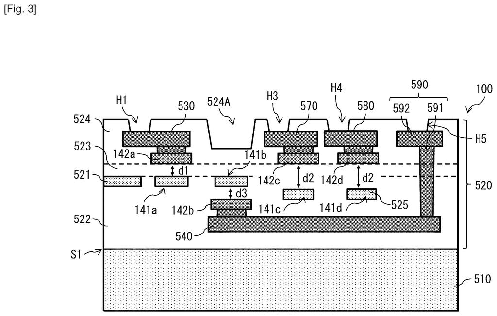
What Sony's waveguide heater chip actually does
Ever tried to use a laser pointer in freezing cold weather and noticed something felt off? Light-based devices are sensitive to temperature, and tiny channels that guide light inside a chip can behave unpredictably when they get too cold or too warm.
Sony's patent describes a chip that solves this by placing a thin metal layer right next to the light-guiding channel, acting as a built-in heater. Instead of relying on the surrounding environment to keep the chip at the right temperature, the chip manages its own heat from within.
This kind of precise temperature control matters most in LiDAR sensors and other optical devices that need to measure distances or detect objects accurately, like those used in cameras, autonomous vehicles, or industrial scanners. Keeping the light channel at a stable temperature means the chip's readings stay consistent even when conditions outside change.
… a first metal film disposed to be opposed to the supporting substrate with the waveguide interposed therebetween, and the first metal film includes a first heater layer configured to serve as a heater for the waveguide.
Translation: A thin metal layer sits right near the light path to warm it up.
How the metal film heats the light channel inside the chip
The patent describes a semiconductor device built as a bonded stack of two layers: a silicon photonics layer on top and a supporting substrate beneath it.
The silicon photonics layer contains a waveguide, which is a narrow channel that carries light signals the way a fiber optic cable carries light, but on a chip. Waveguides are sensitive to temperature changes because heat causes the material to expand slightly, which shifts how light travels through it and can throw off measurements.
Directly above the waveguide sits a metal film that doubles as a heater. The film is positioned on the opposite side of the waveguide from the supporting substrate, sandwiching the light channel between the heater above and the base below. When current passes through that metal layer, it generates heat that warms the waveguide from very close range.
The key engineering detail is the geometry: placing the heater between the waveguide and the outside of the chip, rather than burying it deeper in the stack, lets it heat the waveguide efficiently without wasting energy warming layers that don't need it. The patent claims this integrated approach as a specific structural improvement over attaching heaters externally.
What this means for LiDAR and optical sensor hardware
Temperature control is one of the quieter engineering problems in optical chips. If you have ever seen a LiDAR sensor struggle outdoors in winter or summer, unstable light channels are part of why. A heater built into the chip's own layers eliminates a separate external component and brings the heat source as close to the sensitive channel as physically possible.
For Sony, which already makes image sensors and is several Sony filings on silicon photonics and optical sensing this year, this fits a pattern of building tighter integration between optical and electronic systems on a single chip. Whether it ends up in a consumer camera, a robotics sensor, or something in a car depends on how far Sony takes the design into production.
Sony's 45th filing in the Chip patents we've tracked since May follows work like a noise-canceling sound system and a circuit-packed robot motor.
Getting this from patent to product requires building a new physical chip, not writing a line of code. Sony would need to manufacture a layered silicon structure where a thin metal film acts as a tiny heater, keeping the light-guiding channel inside thermally stable. That is a fabrication challenge measured in years and factory investment, not a software update.
The encouraging detail is that the benefit is immediately measurable. Once a prototype exists, you either see a more stable optical signal across temperatures or you do not. There is no algorithm to tune, no training data to collect.
Sony's sensor business, which already sells on optical precision in real-world conditions, is the most natural destination for something like this. Nothing in this document announces a product, but the engineering problem being solved has an obvious internal customer waiting for it.
There are more where this came from
We read every patent application Big Tech publishes and send you the ones worth knowing. Plain English, free, every week.
The drawings
20 drawing sheets from US 2026/0276814 A1 · click any drawing to enlarge


Want this weekly breakdown for a company we don't cover? Patentlyze Pro →
Be the first to weigh in