
AMD Patents a Technique to Cut Memory Traffic During AI Chip Processing
Moving data around inside a chip burns more power than the math itself. AMD's latest patent targets that hidden cost by rethinking how neural networks shuffle numbers in and out of memory.
What AMD's memory-reduction trick actually does
A chip sits inside a phone or a smart camera, trying to run an AI model. Most of the energy it burns doesn't come from doing the AI math. It comes from constantly fetching and storing numbers in a separate memory chip, over and over again.
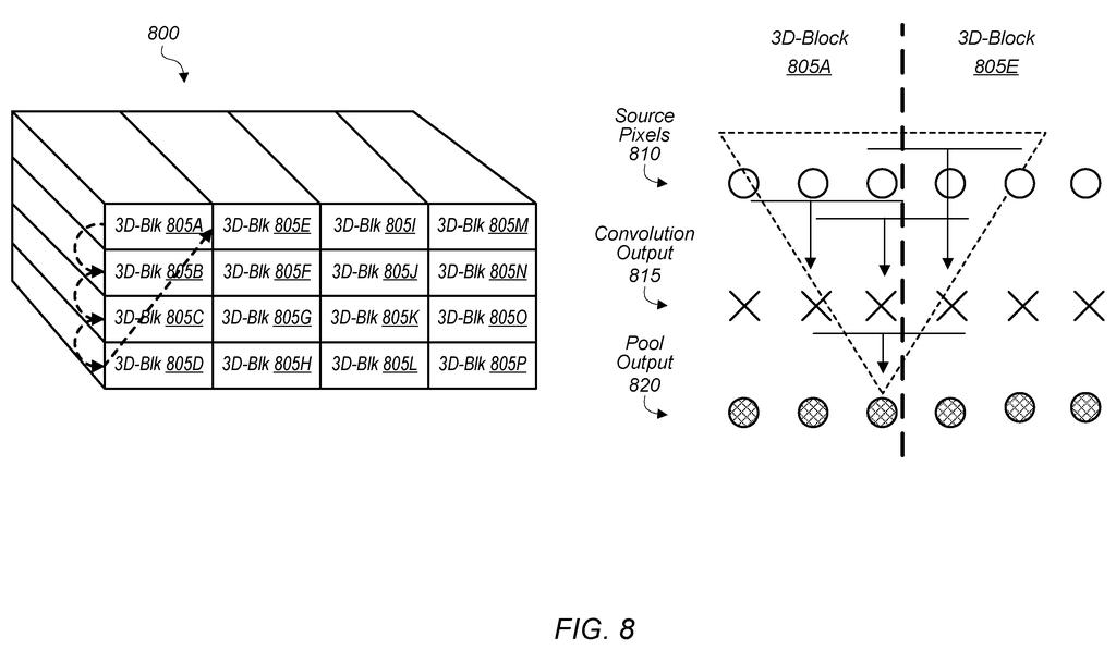
AMD's patent describes a way to cut down that back-and-forth. Instead of pulling data from memory in small chunks and writing results back after every tiny calculation, the system groups the work into compact three-dimensional blocks, does as much as it can on each block while it's already loaded in fast local memory, and only writes the final summed result back to slower external memory.
For you, the upside would be an AI feature, think object detection, image recognition, or voice processing, that runs on a battery-powered device longer without draining the battery as fast. The target here is the kind of low-power chip found in edge devices, not a data-center server.
… add convolution output data together across the first plurality of channels prior to writing the convolution output data to the external memory.
Translation: The chip combines data from multiple channels before saving it back to the main memory.
How AMD slices data into 3D blocks to dodge memory bottlenecks
The patent centers on convolutional neural network (CNN) inference, which is the step where a trained AI model actually processes new data (a photo, an audio clip, a sensor feed) rather than learning from examples.
CNNs process input organized into channels. Think of channels like layers in an image: red, green, and blue are three channels in a standard photo. The chip needs to run a convolution operation (a mathematical sliding-window calculation) across all those channels, and traditionally that means constantly reading from and writing to external memory (a separate RAM chip that is slower and more power-hungry than on-chip storage).
The AMD approach works in three steps:
- Partition input data across all channels into 3D blocks, sized to minimize how often the chip has to go back to external memory.
- Load one block at a time into fast internal (on-chip) memory and run the convolution math there.
- Accumulate (add together) the convolution results across channels before writing anything back out, so only a single final number goes to external memory instead of many intermediate ones.
The key insight is the accumulation step. By summing across channels on-chip first, the system slashes the volume of data that ever touches the slower external bus.
… partitions the input data from the plurality of channels into 3D blocks so as to minimize the external memory bandwidth utilization for the convolution operation being performed.
Translation: Data is chopped into three dimensional blocks to save valuable memory traffic during processing.
What this means for low-power AI chips in everyday devices
Memory bandwidth, how fast and how often a chip can read and write to external RAM, is one of the main limits on running AI at low power. Cutting those trips down means the same calculation costs less energy, which matters most in devices running on batteries or with tight thermal limits.
AMD has been filing around low-power AI inference since at least 2024, and this patent fits that direction. If techniques like this land in a real product, the practical effect for you would be longer battery life on a device that runs local AI tasks, or the ability to run a more capable AI model on hardware that previously couldn't handle it. The patent is filed under ATI Technologies, AMD's GPU subsidiary, so the most likely home for this work is a graphics or AI accelerator chip, not a general-purpose CPU.
AMD's 42nd patent we've tracked since May in our AI chip wars watch builds on one merging AI and graphics and one trimming AI math data.
The core idea here is incremental rather than transformative. Batching memory operations and reducing write-backs is a known strategy in chip design; what this patent describes is a specific implementation shaped around CNN inference workloads on low-power hardware.
From a ship-path perspective, this is not far from real hardware. The technique is largely about how existing memory and compute units are orchestrated, which means it can travel as a firmware or driver-level change rather than requiring new silicon from scratch. That shortens the route to a product considerably.
The honest read is that this is an engineering optimization with a clear commercial target: AI inference on edge devices where power consumption is a hard constraint. It will not change how AI works in any fundamental way, but if it shaves meaningful power off a GPU-class AI accelerator, it earns its place.
There are more where this came from
We read every patent application Big Tech publishes and send you the ones worth knowing. Plain English, free, every week.
The drawings
13 drawing sheets from US 2026/0300709 A1 · click any drawing to enlarge


Want this weekly breakdown for a company we don't cover? Patentlyze Pro →
Be the first to weigh in