
Samsung Patents an Alternating-Voltage Trick to Cut Noise in Camera Sensors
Samsung has filed a patent describing a specific sequence of voltage switches inside an image sensor that could reduce the electronic noise that muddies low-light photos.
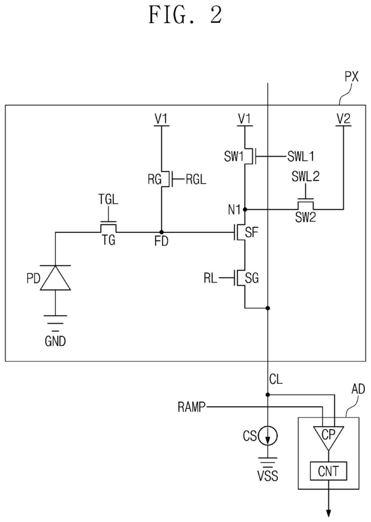
How Samsung's voltage-switching sensor reads light more cleanly
Every camera sensor is haunted by a small amount of random electrical noise, and that noise gets most visible in dark scenes where the signal from actual light is weakest. The sensor has to read out that light signal through a tiny transistor, and the way power is supplied to that transistor can either add to the problem or help cancel it out.
Samsung's patent describes a precise timing sequence: the sensor alternates between two voltage levels while reading your photo. By resetting the circuit at exactly the right moment, catching the light signal, then switching voltage again, the design creates a cleaner baseline for comparison, which makes it easier to separate real light from electrical junk.
The result, in theory, is photos with less grain in shadow areas without needing bigger pixels or a brighter lens.
alternately supplying a first voltage and a second voltage to a first source/drain terminal of a source-follower transistor …
Translation: Switching between two different voltage levels inside the pixel circuit helps clean up unwanted signal interference.
How the source-follower transistor reads two voltages in sequence
The patent centers on a component called a source-follower transistor, a tiny circuit element that amplifies and reads the electrical charge collected by each photodiode (the dot that catches a photon of light). The way this transistor is powered affects how much noise it introduces.
The filing describes a specific sequence:
- Supply a second (lower) voltage to the transistor's supply terminal
- Reset the floating diffusion node (a small charge-storage point between the photodiode and the transistor) to a known reference level
- Switch to a first (higher) voltage
- Transfer the light-collected charge from the photodiode into the floating diffusion node
- Read the voltage at that node through the transistor
- Switch back to the second voltage to finish the cycle
The alternating supply voltage changes the transistor's operating point between the reset step and the signal-read step. This is significant because correlated double sampling (a standard technique that subtracts the reset reading from the signal reading to cancel fixed noise) works better when the transistor's behavior is carefully controlled at each phase.
By tuning what voltage the transistor sees at each moment, Samsung aims to reduce a class of noise called thermal noise and flicker noise that originates inside the transistor itself, not just in the photodiode.
What cleaner sensor readouts mean for phone cameras
For phone cameras, the image sensor is the bottleneck in low light. Manufacturers can add computational tricks after the fact, but cleaner raw data from the sensor always beats trying to recover it in software. A sensor that introduces less noise at the transistor level gives every downstream process, including AI-based night modes, better material to work with.
For consumers, this kind of internal engineering change is invisible in the spec sheet but shows up in real photos. Whether or not this specific approach reaches a shipping product, Samsung's interest in low-noise sensor architecture reflects pressure from customers who judge cameras on how they perform in restaurants and at concerts, not under studio lighting.
Samsung's 141st filing we've tracked since May in our camera sensor push watchlist builds on earlier applications covering two-pass light capture and splitting focus from color pixels.
Samsung filed a patent covering a specific sequence of electrical pulses sent to existing transistors inside an image sensor. No new materials, no new manufacturing process, just a timed control pattern layered onto hardware that camera chips already contain.
That distinction matters for how quickly this could reach a product. Because it lives at the software and circuit-control level rather than requiring a new chip design from scratch, the implementation barrier is lower than most sensor patents. The harder part is validation: a change to readout timing has to be tested across every pixel in a sensor, across heat and cold, before a company ships it in a phone or camera.
If the approach holds up in testing, it fits into a future chip revision rather than demanding a ground-up redesign. That is a realistic path to a shipping product, even if the timeline runs years out.
There are more where this came from
We read every patent application Big Tech publishes and send you the ones worth knowing. Plain English, free, every week.
The drawings
10 drawing sheets from US 2026/0303991 A1 · click any drawing to enlarge


Want this weekly breakdown for a company we don't cover? Patentlyze Pro →
Be the first to weigh in