
Samsung
Samsung · Chip · Filed Dec 4, 2025 · USPTO published Oct 1, 2026 · Oct 1 release
Samsung Patents a Camera Chip That Captures Light in Two Separate Passes
Most camera sensors read all their light-collecting cells at the same moment. Samsung is patenting a design that deliberately staggers that readout, firing a majority group of cells first and a smaller group a moment later, all under a single tiny lens.
- Publication number
- US 2026/0303996 A1(US20260303996A1)
- Applicant
- Samsung Electronics Co., Ltd.
- Filed · Published
- Dec 4, 2025 · Oct 1, 2026
- Inventors
- Dongjin PARK, Jeehong LEE
- Status when we published
- Waiting for an examiner
- Document
- 20 claims
- US classification
- 348/308
What Samsung's two-wave pixel readout actually does
Today's camera image sensors work by having each pixel collect light and then hand that information off all at once. That works fine in bright conditions, but when timing and precision matter, firing every cell simultaneously can cause interference and limit how much creative control the sensor has over what it captures.
Samsung's patent describes a pixel made up of a grid of at least nine light-collecting cells (arranged 3-by-3 or larger), all sharing one tiny lens on top. The trick is that more than half of those cells fire at one moment, and the rest fire at a different moment. Two groups, two timings, one pixel.
The practical benefit is that the sensor can gather more exposure information, reduce certain types of image noise, or enable depth-sensing tricks, because it's pulling light data from the same physical spot in two distinct "snapshots" rather than one. Think of it like taking two rapid photos of the same scene from the exact same position and blending them for a better result.
… P transfer transistors among the first N 2 transfer transistors are configured to be turned on at a time t1 and L transfer transistors among the first N 2 transfer transistors are configured to be turned on at a time t2 different from the time t1 …
Translation: Different groups of microscopic switches turn on at separate moments to capture light in two distinct passes.
How the pixel grid splits into timed transistor groups
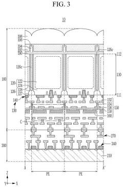
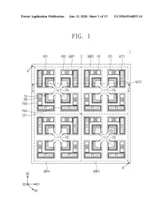
The patent describes an image sensor pixel that contains N-squared photodiodes (light-collecting cells) arranged in an N-by-N grid, where N must be an odd number of at least 3. So the smallest version is a 3×3 grid, giving you 9 photodiodes packed beneath a single microlens (the tiny curved glass dome that focuses incoming light onto the pixel).
Each photodiode has its own transfer transistor, which acts like a gate: when it opens, the charge that light has built up in the photodiode flows out to be measured. The patent's key rule is that these transistors are split into two named groups. The first group, containing more than half of all the transistors, opens at time t1. The second group, containing at least 2 transistors, opens at a different time t2.
Critically, the majority group (called P) must be larger than half of N-squared. So in a 3×3 pixel with 9 total transistors, P must be at least 5. The remaining transistors (called L) are at least 2 but always fewer than P. This asymmetry, a big group and a small group, is the heart of the claim.
- N: grid size (odd, 3 or larger)
- P: the majority transistor group, fires first (t1)
- L: the minority transistor group, fires second (t2)
- One microlens sits over the entire N×N pixel
What this means for camera quality in Samsung devices
Camera sensors are one of the most competitive battlegrounds in consumer electronics, and pixel-level architecture decisions shape everything from how well a phone shoots in dim restaurants to whether it can measure depth for portrait blur. A sensor that reads subsets of a pixel at different times can support phase-detection autofocus, high-dynamic-range capture, or noise reduction without requiring a physically larger pixel.
For you as a consumer, this kind of design is what separates a camera that handles a dimly lit birthday cake from one that turns it into a blurry orange smear. Samsung's bet on sensor architecture suggests the company sees on-chip pixel design, not just software processing, as where the next round of camera improvements will come from.
Samsung's 140th filing we've tracked in our camera sensor push since May builds on work like one splitting focus and color pixels and one for a fridge camera.
Source: US 2026/0303996 A1 at the USPTO (PDF). Full patent text and figures are in the official publication.
Get our take in your Top Stories
Liked this breakdown? Add Patentlyze as a preferred source on Google, and our plain-English take shows up more often in your Top Stories the next time Samsung patent news breaks.
Add Patentlyze on Google
One click.
There are more where this came from
We read every patent application Big Tech publishes and send you the ones worth knowing. Plain English, free, every week.
The drawings · 51 sheets
51 drawing sheets from US 2026/0303996 A1 · click any drawing to enlarge


Show the other 43 sheets


More from Samsung
All 1,662 Samsung patents →
More in Chip
All 649 Chip patents →
Samsung
Samsung Patent Filing Targets Cameras That Adapt Between Bright and Dark Scenes
Samsung
Samsung Patents a Chip-Level Lens That Sorts Light by Color and Direction Simultaneously
Samsung
Samsung Patents a Camera Chip Design That Stops Unwanted Light From Blurring Edges
Samsung
No comments yet