Samsung Patents a Chip Package That Buries Passive Components Inside Camera Modules
Samsung is patenting a way to hide the small resistors and capacitors that normally crowd a circuit board inside the chip package itself — a packaging trick that could shave precious millimeters off camera module height.
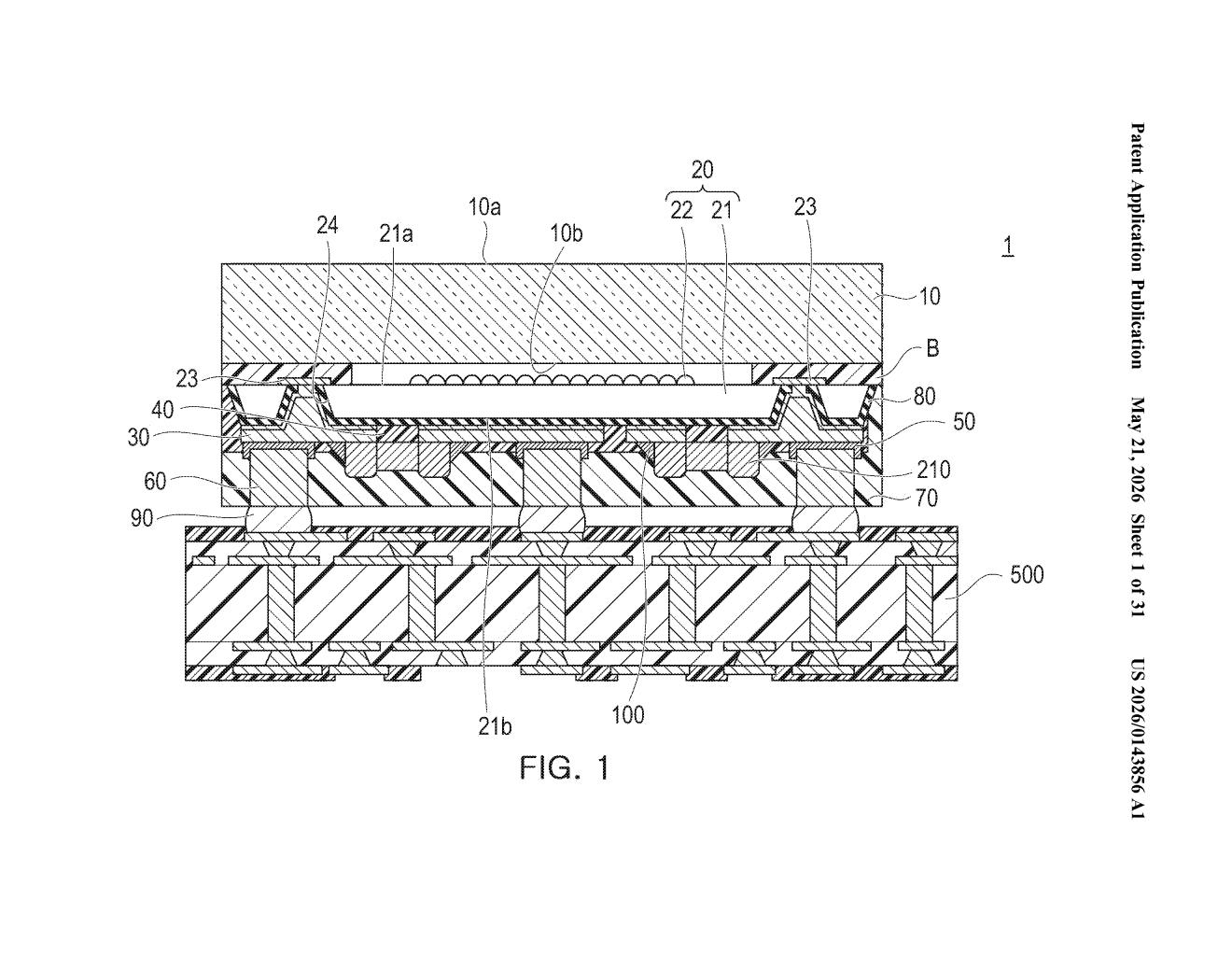
What Samsung's buried-component chip package actually does
Imagine the inside of a smartphone camera. Alongside the main image sensor chip, there are dozens of tiny resistors and capacitors — called passive components — that filter power and signals. Right now, these components typically sit next to the chip on the circuit board, taking up horizontal space and adding height.
Samsung's patent describes a way to tuck those passive components underneath the chip, buried inside a protective resin that seals everything together. The components sit lower than the tall copper pillars (called columnar electrodes) used to connect the package to the rest of the device, so the resin can encapsulate them completely without interfering with those connections.
The result is a more compact, self-contained package — one that routes electrical signals through the chip itself via tiny holes, rather than around the outside. For camera modules in particular, where every tenth of a millimeter counts, this kind of integration can make a real difference.
How the redistribution layer and columnar electrodes stack up
The patent describes a fan-out wafer-level package (FOWLP) — a chip packaging architecture where connections are redistributed across a wider area than the chip's own footprint — combined with embedded passive components.
Here's how the layers stack:
- The image sensor chip sits at the top, with electrodes on its bottom (first) surface.
- Through-hole vias — tiny tunnels drilled through the chip substrate — expose those electrodes to the layer below.
- A redistribution layer (RDL) on the chip's back surface routes those signals outward, acting like a miniaturized printed circuit board bonded directly to the chip.
- Passive components (capacitors, resistors, inductors) are mounted directly on the RDL's outer surface, but sit shorter than the copper columnar electrodes that rise up from the same surface.
- An encapsulating resin fills the space, fully burying the passive components while leaving the tops of the columnar electrodes exposed for external connections.
The key claim is the height relationship: passive components must be shorter than the columnar electrodes relative to the RDL surface, so resin can cover the components without also burying the connection points. It sounds simple, but getting this geometry right in mass production is a real engineering constraint.
What this means for thinner smartphone camera hardware
Thinner smartphone camera bumps are one of the most visible hardware constraints phone makers wrestle with. Embedding passive components inside the package — rather than scattering them on the motherboard — reduces the total area and height the camera module needs. Less board real estate means more room for a larger sensor, a bigger battery, or simply a flatter phone.
For Samsung, which manufactures both the image sensors (via Samsung Semiconductor) and the phones that use them (Galaxy series), this kind of vertical integration of packaging technology is a natural competitive lever. The filing names Japanese inventors, hinting at possible collaboration with or acquisition of specialized packaging expertise from Japan's deep semiconductor supply chain.
This is unglamorous but genuinely useful semiconductor packaging work — the kind of incremental engineering that quietly enables the next generation of slim camera hardware. It won't make headlines at a Galaxy Unpacked event, but packages like this are exactly why modern smartphones can fit three cameras in a body thinner than a pencil.
Get one Big Tech patent every Sunday
Plain English, intelligent commentary, no hype. Free.
Editorial commentary on a publicly published patent application. Not legal advice.