Samsung Patents a Precision Grid Structure for Next-Gen Image Sensors
Samsung is quietly filing patents on the microscopic scaffolding that sits between your camera's color filters — and the geometry of that scaffolding has a surprisingly big effect on image quality.
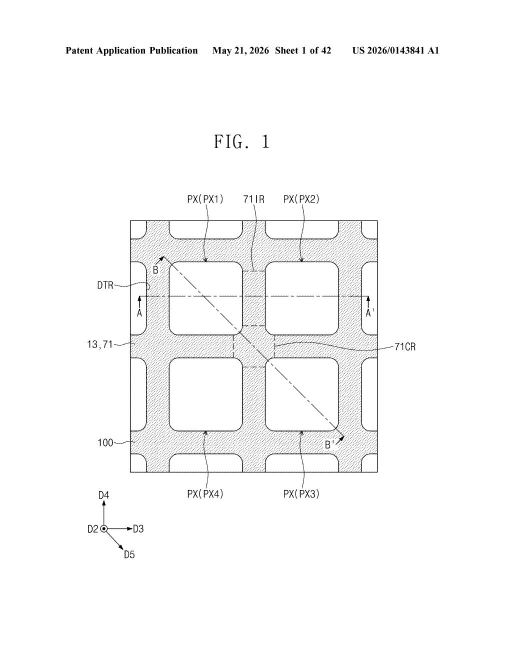
What Samsung's color-filter grid structure actually does
Imagine a camera sensor as a grid of millions of tiny buckets, each catching a different color of light — red, green, or blue. The walls between those buckets matter a lot. If light leaks from one bucket into a neighbor, you get muddy colors and reduced sharpness. That's the problem Samsung is trying to solve here.
This patent describes a specific shape and structure for the dividers — called grid structures — that sit between the color filters in an image sensor. The key trick is a carefully engineered air pocket (the fence gap) inside each divider wall, surrounded by an insulating layer that seals it in a precise way.
The benefit of trapping air in there is that air doesn't transmit light the way solid materials do, so it acts as a better optical barrier. Samsung's patent defines exactly how much of that air pocket must be covered by the insulating layer — at least 50% of the bottom surface — to keep the structure stable without sacrificing its light-blocking performance.
How the fence gap and insulating layer work together
The patent covers a specific architecture for the grid walls that separate color filters on a CMOS image sensor (the chip type used in virtually every smartphone camera today).
Each grid structure contains three key components:
- A fence gap — a precisely shaped hollow cavity inside the wall, with a curved top, two vertical sidewalls, and a flat bottom surface
- A gap insulating layer — a thin material that completely wraps the curved top and both sidewalls of the cavity, and covers at least half of the flat bottom
- A supporter — a separate structural element that sits on top of the insulating layer but is physically isolated from the gap itself
The air inside the fence gap has a very low refractive index (meaning light doesn't bend or pass through it easily), which makes it an effective optical isolator between adjacent color filters. The insulating layer's job is to seal the cavity so it stays stable during manufacturing without collapsing.
The 50%-or-more coverage rule on the bottom surface is the engineering detail that makes this work — enough coverage to hold the structure together, but leaving enough air volume to maintain the optical isolation benefit. The supporter being spaced away from the gap prevents mechanical stress from distorting the cavity's shape.
What this means for Samsung camera sensor quality
Light crosstalk — where photons intended for one pixel bleed into a neighboring one — is one of the core challenges in making smaller, denser image sensors. As pixel sizes shrink (which is how manufacturers pack more megapixels into the same chip area), the walls between pixels get thinner and crosstalk gets worse. A grid structure with an engineered air gap is a known approach to this problem, and the precise geometry Samsung is patenting here is about making that approach manufacturable at scale.
For Samsung's camera sensor business — which supplies chips to its own Galaxy phones as well as external customers — incremental improvements in pixel isolation directly translate to better low-light performance and color accuracy. This is unglamorous but real engineering work.
This is deep-in-the-stack semiconductor fabrication work — not the kind of patent that makes headlines, but exactly the kind that determines whether a camera sensor performs well in dim light. Samsung's sensor division competes hard against Sony's IMX series, and pixel-level optical isolation is a genuine differentiator. Worth a note for anyone tracking camera silicon.
Get one Big Tech patent every Sunday
Plain English, intelligent commentary, no hype. Free.
Editorial commentary on a publicly published patent application. Not legal advice.