
Sony Files Patent to Shrink Tiny Display Panels by Stacking Their Circuitry
Every pixel in a liquid crystal display carries its own little circuit, and Sony's new patent application moves part of that circuit onto a second stacked layer so the chip doesn't have to grow.
What Sony's stacked display pixel actually does
Ever tried to fit a week of clothes into a carry-on? You either leave things behind or you stack them neatly. Sony's engineers faced the same puzzle inside a tiny liquid crystal display, the kind found in projectors, headsets and laser equipment.
Every pixel needs a small circuit that decides how much light to let through, and that circuit has many parts. Lay them all side by side and the chip gets bigger. So Sony's patent application splits the parts across two layers. The liquid crystal and some parts sit in a first layer made from an oxide material, which handles high voltage and leaks very little power. The rest sit in a second layer of ordinary silicon stacked on it.
The payoff is a smaller footprint and, in several versions, faster switching too.
… a first semiconductor layer in which the liquid crystal element and a subset of the plurality of electronic components are disposed; and a second semiconductor layer that is stacked o the first semiconductor layer and in which remaining components of the plurality of electronic components are disposed.
Translation: The display splits its driving circuitry across two vertically stacked silicon layers to save precious footprint space.
How Sony splits a pixel across two layers
The patent application covers a light-controlling panel it calls an electro-optical device. Each pixel holds a liquid crystal element, a tiny cell whose molecules tilt according to a voltage. That tilt sets how much the passing light is modulated (dimmed or bent). A small circuit in every pixel does three jobs: a sampling transistor (a switch that grabs the incoming signal), a buffer circuit (which boosts it), and a transfer transistor (which passes it to the liquid crystal).
The claims put the liquid crystal and some of those parts in a first semiconductor layer, and the remaining parts in a second layer stacked on it. In the described versions, the first layer is an oxide semiconductor (good at high voltage and low leakage) and the second is silicon, where electrons move faster. Using paired transistors called CMOS also cancels switching noise without a spare helper transistor.
The filing describes several ways to divide the work:
- Sampling and transfer switches in silicon, buffer in oxide.
- Only the sampling switch in silicon.
- The buffer in silicon, including a feedback design (a voltage follower) that is less thrown off by transistor variation.
- Two sampling and two transfer switches, so one frame's signal loads while another is shown.
- Splitting the circuit that turns a digital brightness value into the pixel signal.
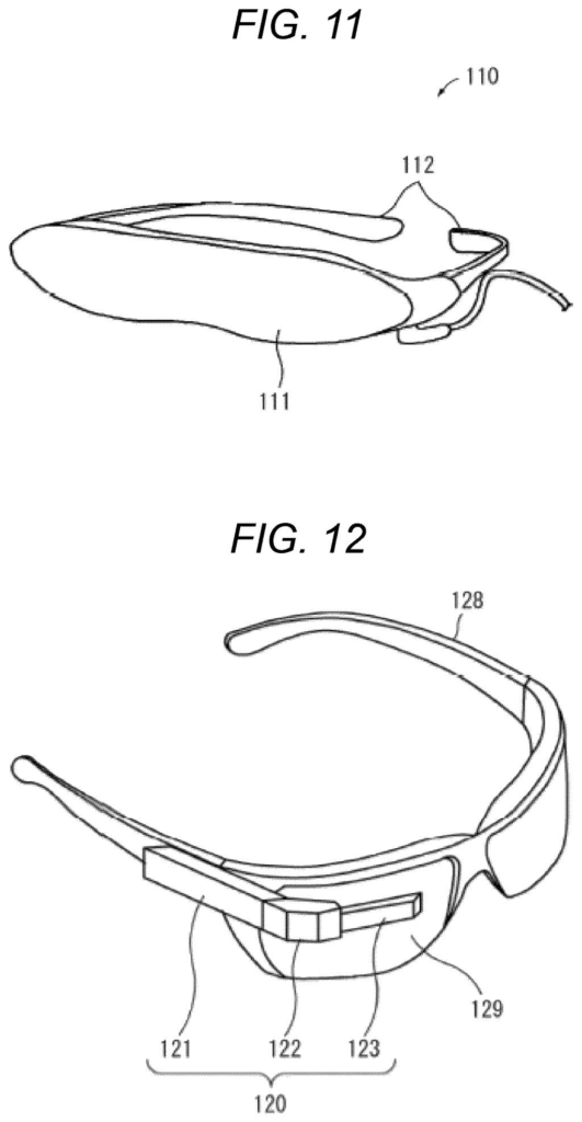
Listed uses include laser processing (with pixels 3.6 micrometers apart or less), optical computing, headsets, camera viewfinders, TVs, phones, car displays and projectors.
An electro-optical device according to the present disclosure includes a liquid crystal element, a plurality of electronic components, a first semiconductor layer, and a second semiconductor layer.
Translation: This miniature screen design relies on a layered architecture of pixels and supporting microchips.
Why smaller display chips matter for headsets
If you wear a headset, look through a camera viewfinder or watch a projector, a smaller display chip is what lets makers shrink or lighten the gear. The filing lists exactly those products, plus car dashboards and laser equipment, as places the stacked design could go.
Speed matters too. Silicon switches faster than the oxide material, and the filing says that cuts the delay in loading each pixel's signal. A patent application is not a product, and the text gives no size or speed figures, so this is best read as a design direction from Sony Semiconductor Solutions, the company's chip arm, rather than something heading to store shelves.
Sony's 95th filing in our Display coverage since May builds on earlier work like one shrinking 3D sensors and one fixing headphone orientation.
Shrinking a display chip sounds minor until you remember that every pixel repeats the same little circuit, and a modern panel has a great many pixels. Saving a sliver of space in one pixel adds up across the whole panel, and panel size drives cost, weight and how small a headset or projector can get.
Sony's answer matches that problem directly: if the parts don't fit side by side, build upward. The filing gives no measurements of how much area this saves, so the size of the win is unknown.
The two-material split makes sense on its own terms. Each part goes in the layer that suits it, and the filing says a few things get faster along the way. Display engineers will care about this far more than shoppers will, and they have a real problem to point at.
Get our take in your Top Stories
Liked this breakdown? Add Patentlyze as a preferred source on Google, and our plain-English take shows up more often in your Top Stories the next time Sony patent news breaks.
There are more where this came from
We read every patent application Big Tech publishes and send you the ones worth knowing. Plain English, free, every week.
The drawings
15 drawing sheets from US 2026/0329139 A1 · click any drawing to enlarge


Show the other 7 sheets


Want this weekly breakdown for a company we don't cover? Patentlyze Pro →
Be the first to weigh in