
Samsung Patents Touchscreen Wiring That Crosses Over Itself Without Shorting Out
Behind the glass of your phone, touch wires near the edge sometimes have to cross each other, and one accidental contact could short them out. Samsung's filing routes one wire underneath the other to prevent that.
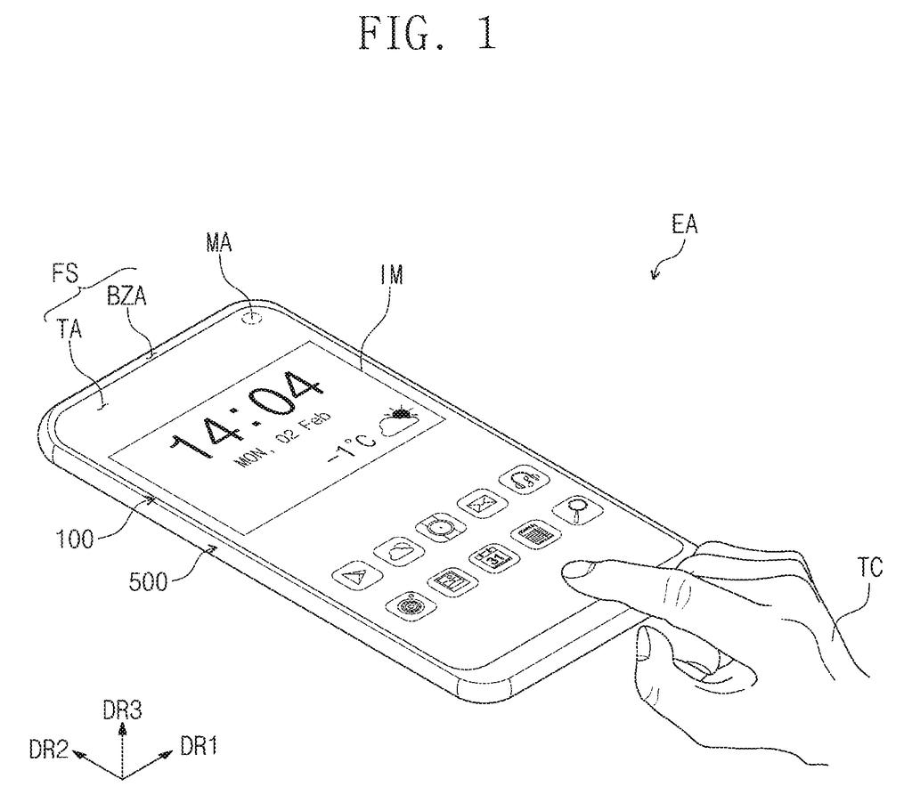
What Samsung's touchscreen border wiring does
Every time you swipe or tap your phone, tiny electrical signals race along thin wires hidden in the border around the screen. Each wire carries a touch from one spot on the glass back to the chip that reads it.
Screens come in all sorts of shapes now, and that forces some of those wires to cross paths. If two wires touch when they shouldn't, you get a short circuit. Samsung's filing solves this by sending one wire underneath the other, on a separate layer with insulation in between.
The lower wire links back up through tiny openings in that insulation. The wire on top gets slots cut into it so the two don't interfere with each other as they cross. You would never see any of this, and you would only notice it if it went wrong.
… the connection line does not overlap the first auxiliary sensing line, crosses the first sensing line in a plan view, and connects the second sensing line to the second sensing pattern through contact holes defined through the insulating layer.
Translation: A bridge connection crosses another line on a different layer to link the touch sensors safely.
How the crossing wire slips under its neighbor
The claim covers an electronic device with a glass window over a display module, which holds a display panel and a touch sensor layer. The touch layer works by measuring tiny changes in capacitance (how much electrical charge a grid can hold) between two sets of electrodes (conductive pads arranged in a grid) when a finger gets close.
The electrodes connect to signal lines in the border. Each line has a backup twin on a lower layer, called an auxiliary line, so a signal can still get through if the main line breaks. The trouble comes when a wire from one electrode set is blocked by a wire from the other set sitting in its way.
The filing's fix is a connection portion on the lower layer. It passes beneath the blocking wire and joins back up through contact holes (small openings in the insulating layer between the two layers). Claim 1 adds specific details:
- The blocking wire has a widened middle section made of several side-by-side strands.
- The backup twin beneath it has a gap, and the connector crosses through that gap.
- The filing says the slots in the wide section reduce coupling (unwanted electrical interference between crossing wires).
Other claims add a wider middle section, a connection electrode at a corner, and a hole through the display with an electronic module underneath.
What this means for touch on odd-shaped screens
The description says the shapes of modern displays force some touch wires to cross, which raises the odds of a short circuit. This layout lets them cross safely. It also works around a hole through the screen with a component underneath, which the filing says can shrink the border around your display.
The patent office has approved this application, and once Samsung pays the final fee it should be issued as a granted patent. It continues a family of filings that traces back to a Korean application from December 2019, and earlier members of that family have already been issued.
Samsung's 129th filing we've tracked since May in our display technology watchlist, it builds on earlier applications like one warming screens at night and one fixing colors as heat rises.
Claim 1 is a long list of specific wiring details, and a product would need every one of them to fall inside it. It names a glass window over a display with a touch layer, a backup wire on a lower layer, a main wire split into several strands in its middle, a gap in the backup, and a connector that passes through that gap. Leave out any piece and the claim does not apply.
That makes the claim narrow. A rival with a different way of routing its touch wires, or one that skips the backup wire entirely, would likely fall outside it. If issued, it would cover a device built with this exact crossing arrangement.
As a story for your next phone, it is a small one. You will never see these wires, and the best result is that nothing about your touchscreen changes. For Samsung's display business, a tight claim on a specific fix for a specific failure is a sensible thing to hold.
Get our take in your Top Stories
Liked this breakdown? Add Patentlyze as a preferred source on Google, and our plain-English take shows up more often in your Top Stories the next time Samsung patent news breaks.
There are more where this came from
We read every patent application Big Tech publishes and send you the ones worth knowing. Plain English, free, every week.
The drawings
17 drawing sheets from US 2026/0349567 A1 · click any drawing to enlarge


Show the other 9 sheets


Want this weekly breakdown for a company we don't cover? Patentlyze Pro →
Be the first to weigh in