Samsung Patents a DC-DC Converter That Bleeds Off Dangerous Voltage Spikes in Storage Chips
Voltage spikes inside storage chips are silent killers — they can corrupt data or fry sensitive circuits before any software layer can respond. Samsung's new patent describes a power management circuit with a built-in escape valve that safely bleeds off excess voltage before it becomes a problem.
What Samsung's overvoltage protection circuit actually does
Imagine a water pipe with a pressure relief valve. Under normal conditions, the valve stays shut and water flows normally. But if pressure suddenly surges — say, a pump kicks on too hard — the valve opens just enough to let the excess pressure escape safely, protecting the pipes downstream.
That's essentially what Samsung's new power management circuit does for the voltage supply inside a storage device. Under normal operating conditions, it regulates voltage the usual way: two switches flip on and off rapidly to keep the power level within a safe range. But if the voltage suddenly spikes above a safe ceiling, a third switch kicks in — one that routes excess electrical charge back through a resistor, slowing the discharge and preventing a damaging surge.
The end result is a chip that can protect itself from overvoltage events without needing external components or software intervention. For you as a user, that kind of built-in resilience is what separates storage that lasts years from storage that fails unexpectedly.
How the three-switch topology handles normal and spike conditions
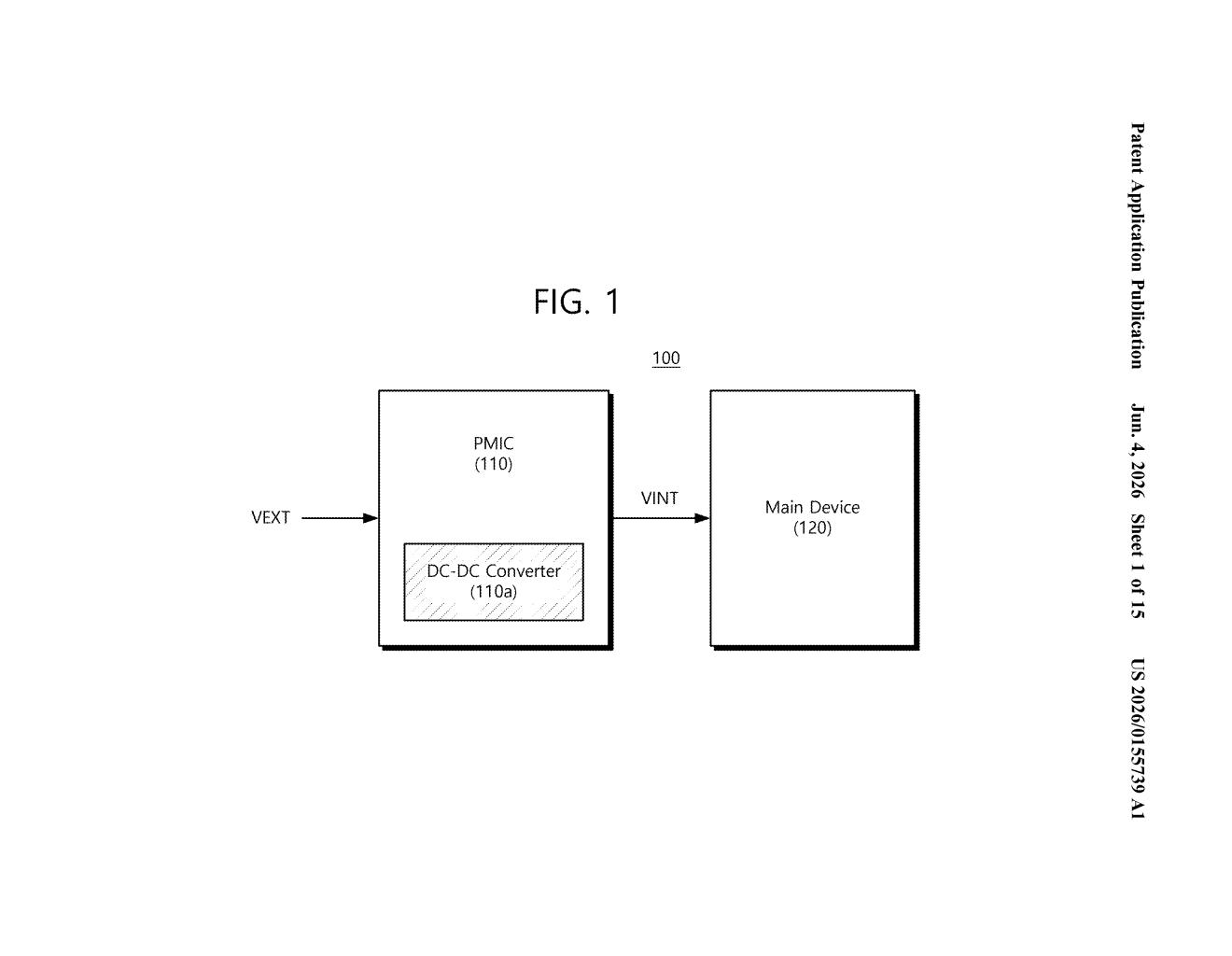
The patent describes a power management integrated circuit (PMIC) designed for storage devices — think SSDs or embedded flash memory. Its core job is to take an external supply voltage and convert it into a stable internal voltage that sensitive memory circuits can use.
The DC-DC converter at the heart of the design uses three switches arranged around a central node:
- Switch 1 connects the external supply voltage to the output node — it's the "fill" switch that pushes current in.
- Switch 2 connects the output node to ground — it's the "drain" switch that pulls current out.
- Switch 3 connects the external supply back to the output node, but through a resistor — it's the overvoltage relief path.
A pulse width modulation (PWM) control circuit (a controller that varies how long each switch stays on to regulate voltage) monitors the internal voltage level and decides which pair of switches to activate.
During normal operation, Switches 1 and 2 alternate to keep the voltage oscillating between two safe reference levels. If the voltage climbs above the upper reference — an overvoltage event — the PWM controller deactivates Switch 1 and activates Switches 2 and 3 instead. The resistor in Switch 3's path limits how fast current flows back in, preventing a destructive oscillation while still pulling the voltage back down to the safe lower reference. A downstream voltage distribution circuit then converts this intermediate voltage into the final supply rail used by the storage chip.
What this means for NAND storage reliability at scale
Storage chips — especially high-density NAND flash — operate within tight voltage windows. An overvoltage event that exceeds those windows even briefly can cause write errors, accelerate wear, or permanently damage the memory array. Traditional DC-DC converters handle overvoltage clumsily: they either cut power entirely (disruptive) or rely on external protection components (costly and slow). Samsung's approach adds a third-switch relief path directly inside the converter, making the response faster and the design more integrated.
For enterprise SSDs and embedded storage in devices like smartphones and servers, tighter on-chip power management means fewer failure modes and potentially longer endurance. It's the kind of unglamorous engineering that doesn't show up in a spec sheet but quietly determines whether a product survives years of real-world use.
This is deeply unsexy infrastructure work — three switches and a resistor — but the engineering insight is genuinely clean. Adding a resistor-limited third path inside the converter itself is a more elegant solution to overvoltage protection than bolting on external clamps or relying on firmware shutdowns. Samsung files a lot of power management patents, and this one looks like the kind of quiet improvement that ends up in every future SSD controller revision.
Get one Big Tech patent every Sunday
Plain English, intelligent commentary, no hype. Free.
Editorial commentary on a publicly published patent application. Not legal advice.