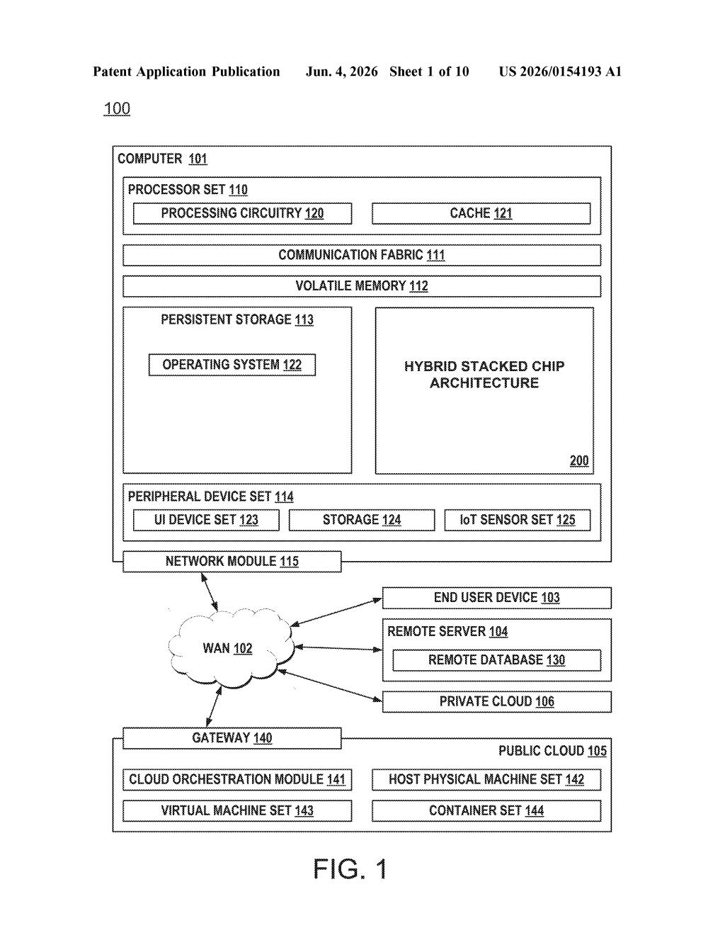
IBM Patents a Chip Stack That Combines Fast DRAM and Flash Storage
IBM is patenting a memory architecture that physically stacks fast DRAM chips together with NAND flash storage in a single package — blurring the line between memory and storage at the hardware level.
What IBM's hybrid memory stack actually does
Imagine your computer's memory (the fast, short-term kind) and storage (the slower, long-term kind) living in the same tiny physical chip sandwich rather than on opposite ends of a motherboard. That's basically what IBM is describing here.
Right now, fast DRAM and high-capacity NAND flash are separate components, often far apart inside a system. IBM's patent describes a chip stack where multiple DRAM chips and a NAND flash chip are all physically stacked on top of each other and wired together. When something requests data, the system can pull from either the speedy DRAM layers or the denser flash layer — all within the same compact package.
The practical upside is density plus speed in a smaller footprint. You get the rapid-access benefits of DRAM alongside the storage capacity of flash, without the long physical distance data normally has to travel between them.
How DRAM and NAND flash share a single chip stack
The patent describes an apparatus — physical hardware — built around a substrate (think of it as the base board that everything mounts onto). Stacked vertically on that substrate are multiple DRAM chips (Dynamic Random-Access Memory — the fast, volatile memory your CPU uses for active workloads) plus at least one NAND flash chip (the same non-volatile storage technology used in SSDs and USB drives, which holds data even when power is off).
The key architectural claim is that the NAND flash chip is inside the same chip stack as the DRAM, and is directly communicably coupled to the DRAM chips — meaning they can talk to each other over very short, high-bandwidth connections rather than routing data across a PCB or through a memory controller sitting elsewhere on the board.
When a request comes in for data, the system accesses it through the unified stack, drawing from whichever layer holds the relevant data:
- DRAM layers for fast, frequently accessed working data
- NAND flash layer for higher-capacity, persistent storage
- The substrate as the interface to the rest of the system
This is architecturally similar in spirit to High Bandwidth Memory (HBM) stacking — where multiple DRAM dies are stacked using through-silicon vias — but here IBM is mixing memory types rather than just stacking identical DRAM dies.
What this means for high-bandwidth memory design
The gap between memory bandwidth and storage capacity is a persistent bottleneck in data-intensive computing — AI inference, database workloads, and large-scale data analytics all suffer when fast memory runs out and the system has to reach far for more data. Putting NAND flash inside the memory stack shortens that physical and logical distance considerably, potentially letting systems treat a larger pool of storage-class memory as near-DRAM-speed capacity.
For IBM, which sells heavily into enterprise and AI infrastructure, this kind of architecture could show up in future server memory modules or AI accelerator designs where maximizing data throughput per watt and per unit of board space matters enormously. It also fits into a broader industry trend of storage-class memory — the idea that the boundary between RAM and storage should be a gradient, not a wall.
This is a genuinely interesting architectural patent, not a routine filing. Mixing DRAM and NAND flash in the same physical stack is a meaningful design bet — it trades the clean separation of memory and storage for tighter integration and potentially higher effective bandwidth. IBM is one of the few companies with both the chip design chops and the enterprise customer base to actually productize something like this, so it's worth watching.
Get one Big Tech patent every Sunday
Plain English, intelligent commentary, no hype. Free.
Editorial commentary on a publicly published patent application. Not legal advice.