
Samsung Patents AI That Fixes Chip-Printing Template Errors Before Manufacturing
Every modern chip starts life as a photographic stencil, and a single flaw in that stencil can ruin an entire batch of processors. Samsung is training an AI to catch and fix those flaws automatically before a single wafer is exposed to light.
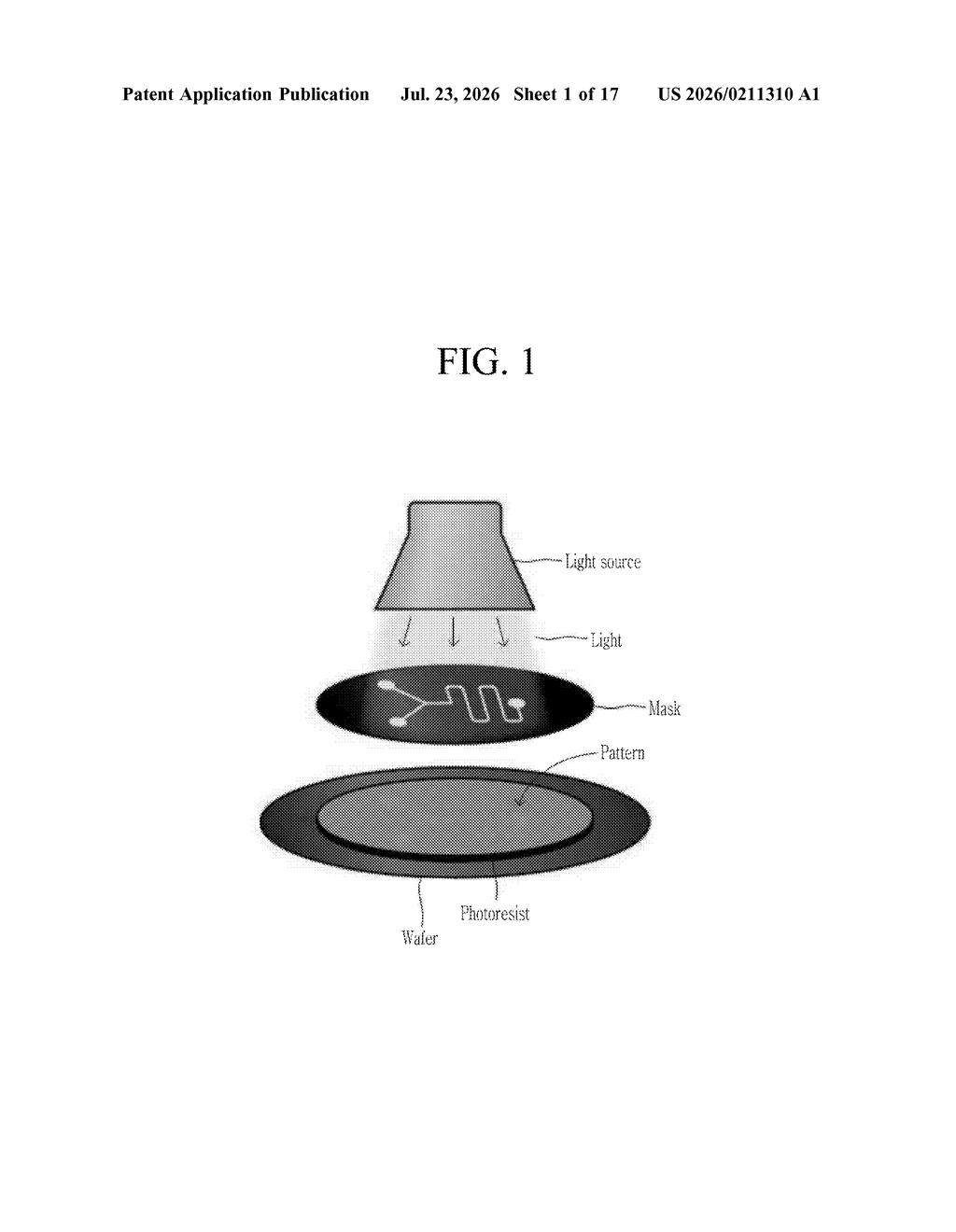
What Samsung's AI mask-correction system actually does
Imagine printing a trillion-piece puzzle onto a silicon wafer using light. The 'stencil' that guides that light, called a photomask, has to follow extremely strict geometric rules. Even tiny violations of those rules can cause the wrong circuit pattern to appear on the chip, leading to defects.
Traditionally, engineers use software called optical proximity correction (OPC) to prepare these stencils, then run additional checks to catch any rule violations. It's a slow, iterative process. Samsung's patent describes training an AI model specifically to spot those violations in the corrected stencil image and fix just the problem areas, without touching the rest.
The result is a corrected mask image that passes all the rules without requiring engineers to manually loop back through the correction process. It's a bit like having a spell-checker that not only flags errors but rewrites the offending sentences for you.
How the correction network finds and fixes mask violations
The patent describes a three-step pipeline running on a processor:
- Step 1, OPC image generation: Standard optical proximity correction software produces a first mask image. OPC pre-distorts the stencil shapes so that, after light diffracts through them, the pattern on the wafer comes out correct. But OPC doesn't guarantee the resulting mask shapes satisfy all manufacturing rules.
- Step 2, Correction network training: A neural network (called a 'correction network') is trained specifically to identify regions in the mask image that violate mask rules (think of these as geometric design laws about minimum feature sizes, spacing, or shape complexity). The network learns what a rule-compliant version of those regions should look like.
- Step 3, Inference: The trained network takes the rule-violating mask image and outputs a corrected version with no remaining violation points.
The USPC classification (430/5) places this squarely in photomask and microlithography territory, confirming this is about semiconductor fabrication, not image editing in any consumer sense. The key innovation is using a learned model to handle the correction pass rather than running the full OPC loop again, which is computationally expensive.
What this means for chip manufacturing efficiency
Chip manufacturing is under constant pressure to shrink feature sizes and speed up production cycles. Every time OPC produces a mask with rule violations, engineers either fix it manually or rerun the correction software, both of which cost time and compute resources. An AI that patches violations in a single forward pass could meaningfully reduce that turnaround time.
For Samsung, which both manufactures its own chips and operates one of the world's largest contract foundries, faster mask preparation means faster time-to-yield for new chip designs. If this approach proves reliable enough to reduce or eliminate manual review cycles, it becomes a quiet but real competitive advantage in a market where tape-out schedules are measured in weeks.
This is unglamorous but genuinely useful semiconductor automation. The mask correction step is a real bottleneck in chip design, and applying a trained neural network to it is a logical move that several chip-tool companies are also pursuing. Samsung filing this suggests they want to keep that capability in-house rather than relying entirely on EDA vendors like Synopsys or Cadence.
There are more where this came from
We read every patent application Big Tech publishes and send you the ones worth knowing. Plain English, free, every week.
The drawings
17 drawing sheets from US 2026/0211310 A1 · click any drawing to enlarge


Want this weekly breakdown for a company we don't cover? Patentlyze Pro →
Be the first to weigh in