Amazon Patents a System That Directs AI Tasks to the Right Chip Automatically
Running AI models efficiently means knowing which chip should handle which job — and Amazon wants that decision made in hardware, not software.
What Amazon's mixed-chip AI scheduler actually does
Imagine a kitchen with two kinds of stoves — one for slow-braising, one for high-heat searing. A smart head chef routes each dish to the right burner automatically, so nothing waits in the wrong queue. Amazon's patent describes a similar idea, but for AI chips inside a data center.
Different AI chips are often good at different things. Some are built for a particular style of math-heavy AI work; others handle different instruction formats. Today, making them cooperate usually requires a lot of software overhead. Amazon's approach wants to handle that routing directly in the chip circuitry itself — faster and with less coordination cost.
The result is a system where a piece of AI software can be written once, compiled into instructions for multiple chip types, and then sent automatically to whichever chip is best suited — all without the programmer needing to manage the details by hand.
How the scheduler reads instruction bits to pick the right chip
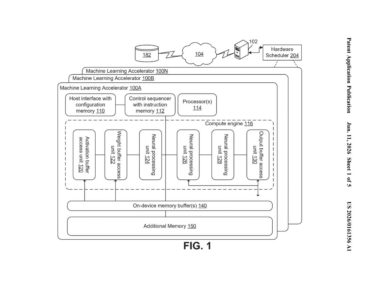
The patent describes a system with two (or more) neural network accelerator tiles — think of each tile as a specialized compute block inside an AI chip. Each tile has its own set of multiply-accumulate units (the fundamental math circuits that do the heavy lifting in neural network calculations like multiplying weights and summing results).
What makes this interesting is how the tiles decide what to do. Rather than relying on a central software controller, each tile reads specific bits embedded in the instruction itself to figure out which of its internal compute units to use. The scheduler circuitry at a higher level does the same thing — it reads bits in an incoming instruction to decide which tile should even receive the job.
Meanwhile, a compiler (software that translates human-readable AI code into chip-level commands) produces two flavors of instructions:
- Instructions formatted for the first chip type (its ISA, or instruction set architecture — the chip's native language)
- Instructions formatted for the second chip type's ISA
The scheduler then routes each instruction to the right destination automatically. The key claim is that this decision-making happens in dedicated hardware circuitry, not in a software loop — which means lower latency and less CPU overhead when dispatching AI workloads.
What this means for Amazon's custom AI silicon strategy
Amazon operates AWS, the world's largest cloud computing platform, and has been aggressively developing its own AI chips — most notably the Trainium and Inferentia series. As AI workloads grow more complex, data centers increasingly mix different chip generations and architectures in the same system. A hardware-level scheduler that can bridge those differences without software glue would be a real operational advantage at Amazon's scale.
For you as a cloud customer, the practical upshot is potentially more efficient — and cheaper — AI inference and training jobs, because Amazon could pack more varied hardware into a single system and use all of it well. It also signals that Amazon is betting on heterogeneous chip designs as the future of its AI infrastructure, rather than standardizing on a single architecture.
This is unglamorous but important plumbing work. The race to build custom AI silicon is well underway at Amazon, Google, and Microsoft — and the companies that solve the chip-coordination problem in hardware rather than software will have a real throughput edge. This patent is a concrete signal that Amazon is thinking about that problem at the architectural level.
Get one Big Tech patent every Sunday
Plain English, intelligent commentary, no hype. Free.
Editorial commentary on a publicly published patent application. Not legal advice.